Semiconductor device

A semiconductor and main body technology, applied in semiconductor devices, semiconductor/solid-state device manufacturing, electrical components, etc., can solve problems such as the inability to fully eliminate the compromise between withstand voltage and on-voltage, and the difficulty of expanding the depletion layer.

Active Publication Date: 2018-01-30
SANKEN ELECTRIC CO LTD
View PDF5 Cites 0 Cited by
  • Summary
  • Abstract
  • Description
  • Claims
  • Application Information

AI Technical Summary

Problems solved by technology

In addition, the method of disposing a carrier storage layer with an impurity concentration higher than that of the drift region in a semiconductor device has the following problems: it is difficult to expand the depletion layer satisfactorily, and the trade-off between breakdown voltage and on-voltage cannot be sufficiently eliminated.

Method used


Image

  • Semiconductor device
  • Semiconductor device
  • Semiconductor device

Examples


Embodiment Construction

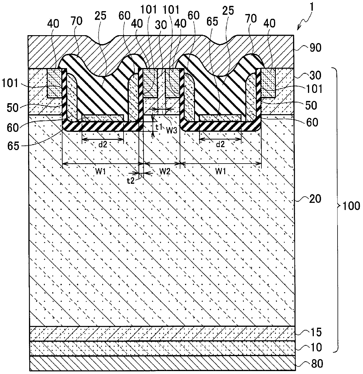
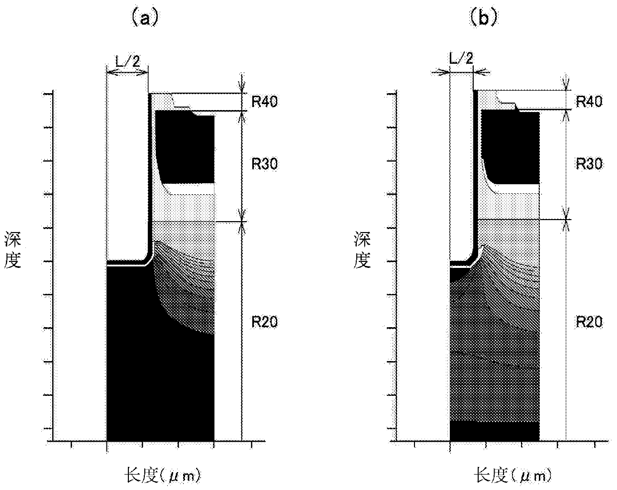
[0033] Next, embodiments of the present invention will be described with reference to the drawings. In the following description of the drawings, the same or similar reference numerals are assigned to the same or similar parts. In addition, it should be noted that the drawings are only schematic, and the relationship between the thickness and the plane size, the ratio of the length of each part, and the like are different from the actual ones. Therefore, specific dimensions should be judged with reference to the following description. In addition, it is needless to say that the drawings include parts where the relationship or ratio of dimensions is different from each other.

[0034] In addition, the embodiments shown below are merely examples of devices or methods for actualizing the technical idea of ​​the present invention, and the technical idea of ​​the present invention does not specify the shape, structure, arrangement, etc. of the components as described below. conte...


PUM


Abstract

The present invention has: a first semiconductor region of the first conductivity type; a second semiconductor region of the second conductivity type disposed above the first semiconductor region; a third semiconductor region of the first conductivity type disposed on the second semiconductor region above the region; the second conductivity type 4th semiconductor region, which is arranged above the 3rd semiconductor region; the insulating film, which is arranged on the inner wall of the groove, and the groove extends from the upper surface of the 4th semiconductor region and penetrates the 3rd semiconductor region. 4. The semiconductor region and the third semiconductor region reach the second semiconductor region; the control electrode is arranged on the insulating film on the side of the groove and faces the third semiconductor region; the first main electrode is electrically connected to the first semiconductor region ; the second main electrode, which is electrically connected to the fourth semiconductor region; and the bottom electrode, which is arranged above the insulating film on the bottom surface of the groove, and the bottom electrode is arranged to be separated from the control electrode, and when viewed from above, the groove is extending The length in the direction is greater than the width of the groove, and the width of the groove is wider than the interval between the grooves adjacent to each other.

Description

technical field [0001] The present invention relates to the structure of a trench gate type semiconductor device performing a switching operation. Background technique [0002] Insulated gate bipolar transistors (IGBTs) have high input impedance and low ON voltage, and thus are used in motor drive circuits and the like. However, in IGBTs, there is a trade-off relationship between breakdown voltage and on-voltage. [0003] Therefore, in order to reduce the on-voltage while maintaining a high withstand voltage, various methods have been proposed. For example, a structure has been proposed in which an n-type layer having an impurity concentration higher than that of the drift region and storing holes (hereinafter referred to as "carrier storage layer") is formed between the base region and the drift region. According to this structure, holes from the collector region can be prevented from reaching the emitter electrode, and the ON voltage can be reduced (for example, refer to...

Claims


Application Information

Patent Timeline
Patent Type & Authority Patents(China)
IPC IPC(8): H01L29/78H01L21/28H01L21/336H01L29/41H01L29/417H01L29/423H01L29/739
CPCH01L21/28H01L29/41H01L29/417H01L29/423H01L29/41708H01L29/4236H01L29/42368H01L29/42376H01L29/4238H01L29/0692H01L29/1095H01L29/407H01L29/7397H01L29/78H01L29/42304
Inventor 川尻智司小川嘉寿子
Owner SANKEN ELECTRIC CO LTD
Why Eureka
Try Eureka