Low-temperature polycrystalline silicon flat panel detector pixel circuit and flat panel detection method
A flat-panel detector and low-temperature polysilicon technology, applied in the field of flat-panel detection, can solve problems such as threshold voltage drift, electrical signal loss, etc., and achieve the effects of reducing off-state leakage current, suppressing electrical signal loss, and high field-effect mobility
- Summary
- Abstract
- Description
- Claims
- Application Information
AI Technical Summary
Problems solved by technology
Method used
Image
Examples
Embodiment 1
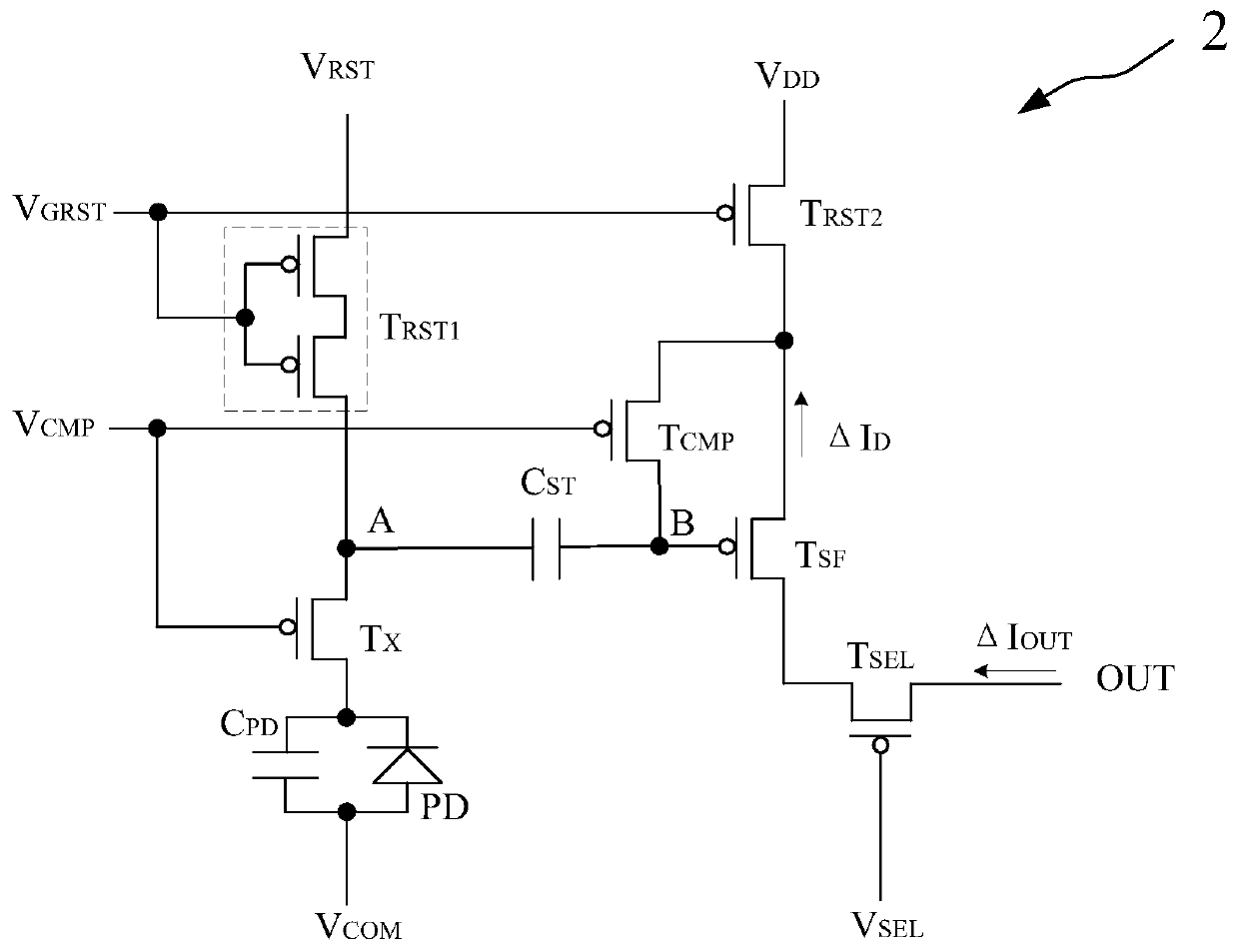
[0051] Such as image 3 As shown, this embodiment provides a low temperature polysilicon flat panel detector pixel circuit 2, the low temperature polysilicon flat panel detector pixel circuit 2 includes: a first reset switch T RST1 , storage capacitor C ST , transmission gate T X , photodiode PD, second reset switch T RST2 , compensation switch T CMP , source follower T SF and selector switch T SEL .
[0052] Wherein, the first reset switch T RST1 The first terminal is connected to the reset signal V RST , the control terminal is connected to the first control signal V GRST , the second terminal is connected to the storage capacitor C ST the first plate of
[0053] The transmission gate T X The first terminal of the storage capacitor C is connected ST The first plate, the control terminal is connected to the second control signal V CMP , the second terminal is connected to the cathode of the photodiode PD, and the anode of the photodiode PD is connected to the bia...
Embodiment 2
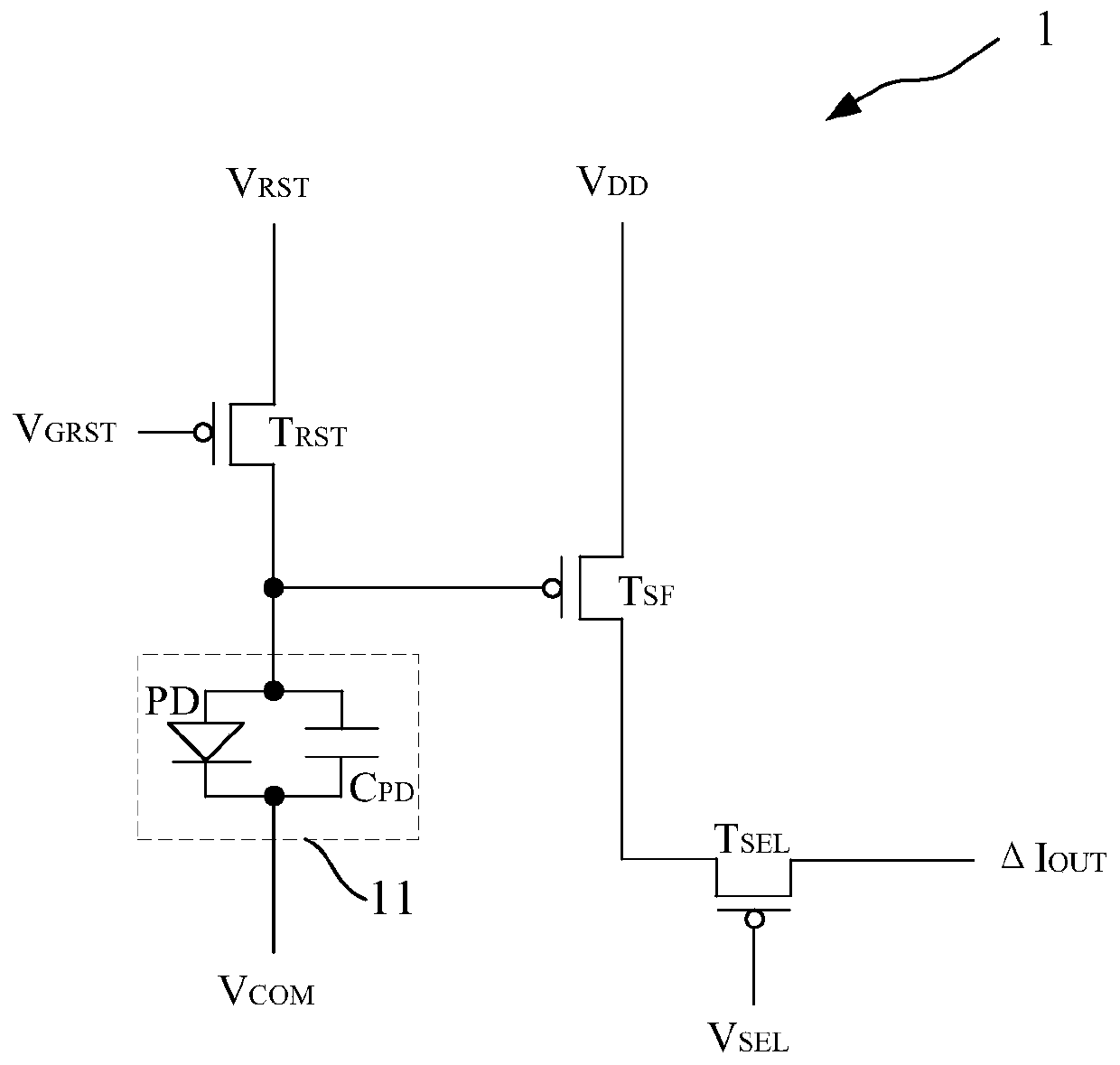
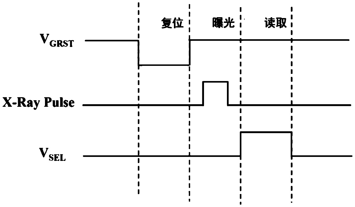
[0064] Such as Figure 4 ~ Figure 8 As shown, this embodiment provides a flat-panel detection method, which is implemented based on the pixel circuit of the low-temperature polysilicon flat-panel detector in Embodiment 1. The flat-panel detection method includes:
[0065] 1) Reset stage: close the selection switch T SEL , turn on the first reset switch T RST1 , transmission gate T X , the second reset switch T RST2 , compensation switch T CMP and source follower T SF ;Storage capacitor C ST The potential on the first plate is reset to a positive level, and the potential on the second plate is reset to a negative level; the photodiode PD is in a reverse bias state.
[0066] Specifically, such as Figure 4 and Figure 5 As shown, in this embodiment, the third control signal V SEL set high, the selector switch T SEL off; the first control signal V GRST and the second control signal V CMP set low, the first reset switch T RST1 , the transmission gate T X , the second...
PUM
 Abstract
Description
Claims
Application Information
 - R&D
- Intellectual Property
- Life Sciences
- Materials
- Tech Scout
- Unparalleled Data Quality
- Higher Quality Content
- 60% Fewer Hallucinations
Browse by: Latest US Patents, China's latest patents, Technical Efficacy Thesaurus, Application Domain, Technology Topic, Popular Technical Reports.
© 2025 PatSnap. All rights reserved.Legal|Privacy policy|Modern Slavery Act Transparency Statement|Sitemap|About US| Contact US: help@patsnap.com


