Normally-equipped integrated unit diode chip
A technology of integrated units and diodes, applied in electrical components, semiconductor devices, circuits, etc., can solve the problems of LED chip light output efficiency and excessive influence of current diffusion, and achieve improved light extraction efficiency, weak light absorption ability, and increased light output area. Effect
- Summary
- Abstract
- Description
- Claims
- Application Information
AI Technical Summary
Problems solved by technology
Method used
Image

Examples
Embodiment 1
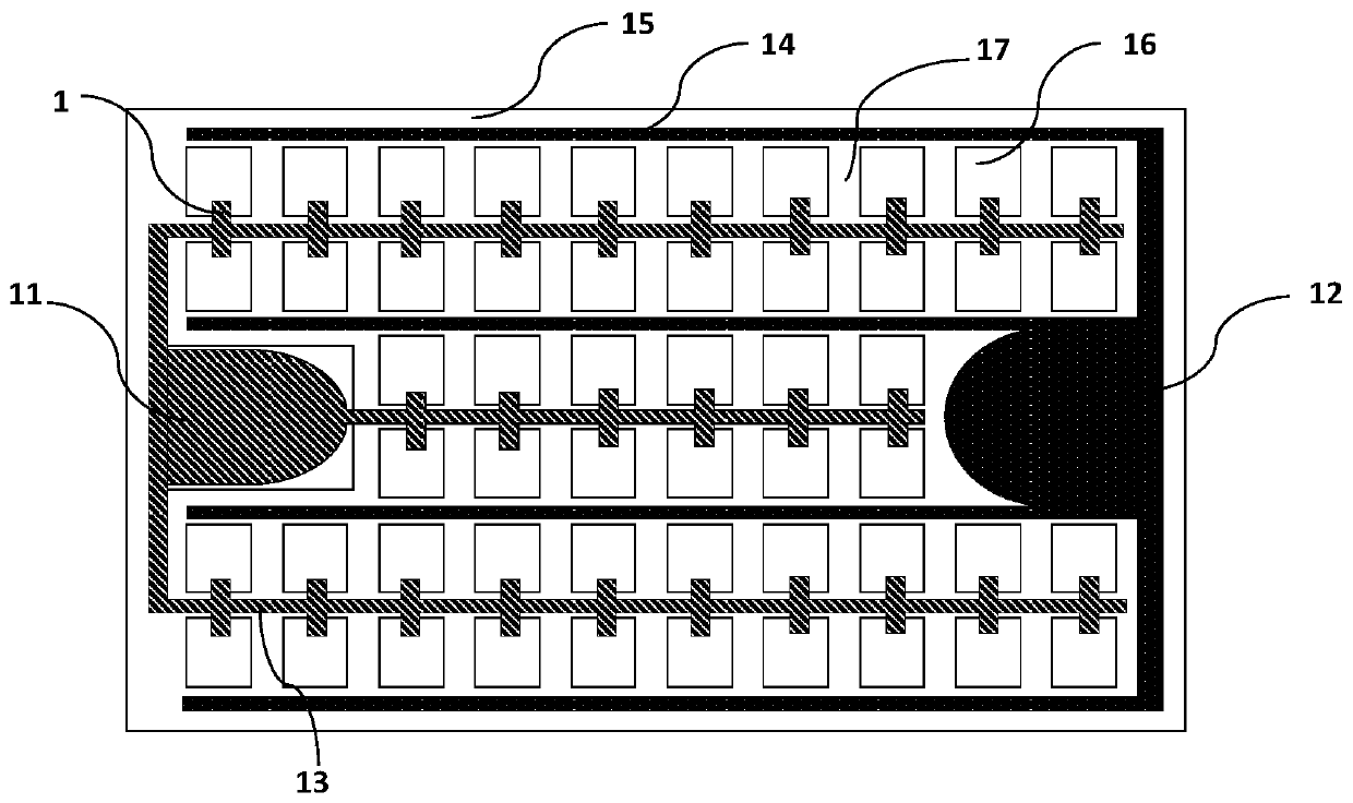
[0037] The present embodiment provides a formally mounted integrated unit diode chip, such as image 3 As shown, it includes: n-type electrode 1 , n-type pad 11 , p-type pad 12 , n-type electrode line 13 , p-type electrode line 14 , diode mesa structure 15 , diode unit 16 and trench 17 . The diode mesa structure includes 6 rows of 52 square diode units 16 of equal size and uniform distribution, and the length of the diode units along the Y-axis direction is 40 microns. The diode mesa structure adopts a square arrangement, and the size of the mesa structure is smaller than the diffusion length of the current injection. The shape of the diodes is a regular rectangle, and they are arranged in a uniform and symmetrical arrangement.
[0038] In some preferred embodiments, the length of the diode unit along the Y-axis direction is 100 nanometers; in other preferred embodiments, the length of the diode unit along the Y-axis direction is 10 nanometers.
[0039] The electrode wires o...
Embodiment 2
[0044] The present embodiment provides a formally mounted integrated unit diode chip, such as Figure 4 As shown, it includes: a first conductivity type electrode 1, a first conductivity type pad 11, a second conductivity type pad 12, a first conductivity type electrode line 13, a second conductivity type electrode line 14, a diode mesa structure 15, a diode cell 16 and trench 17 . The diode mesa structure includes 6 rows of 102 triangular diode units 16 of equal size and uniform distribution, and the length of the diode units along the Y-axis direction is 80 microns. The diode mesa structure adopts a triangular arrangement, and the size of the mesa structure is smaller than the diffusion length of the current injection. The diode units are triangular in shape and distributed according to a uniform symmetrical arrangement.
[0045] In some preferred embodiments, the length of the diode unit along the Y-axis direction is 100 microns; in other preferred embodiments, the length...
Embodiment 3
[0051] The present embodiment provides a formally mounted integrated unit diode chip, such as Figure 5As shown, it includes: a first conductivity type electrode 1, a first conductivity type pad 11, a second conductivity type pad 12, a first conductivity type electrode line 13, a second conductivity type electrode line 14, a diode mesa structure 15, a diode cell 16 and trench 17 . The diode mesa structure includes 6 rows of 52 square diode units 16 of equal size and uniform distribution, and the length of the diode units along the Y-axis direction is 40 microns. The diode mesa structure adopts a square arrangement, and the size of the mesa structure is smaller than the diffusion length of the current injection. The shape of the diode units is a regular rectangle, distributed according to a uniform symmetrical arrangement. Each diode unit is provided with a hole structure, and the hole structure includes two hole units, and the hole unit is a circular hole unit with a diamete...
PUM
| Property | Measurement | Unit |
|---|---|---|
| thickness | aaaaa | aaaaa |
| thickness | aaaaa | aaaaa |
| width | aaaaa | aaaaa |
Abstract
Description
Claims
Application Information
 - Generate Ideas
- Intellectual Property
- Life Sciences
- Materials
- Tech Scout
- Unparalleled Data Quality
- Higher Quality Content
- 60% Fewer Hallucinations
Browse by: Latest US Patents, China's latest patents, Technical Efficacy Thesaurus, Application Domain, Technology Topic, Popular Technical Reports.
© 2025 PatSnap. All rights reserved.Legal|Privacy policy|Modern Slavery Act Transparency Statement|Sitemap|About US| Contact US: help@patsnap.com