Solar cell and manufacturing method thereof
A solar cell and electrode technology, applied in the direction of final product manufacturing, sustainable manufacturing/processing, circuits, etc., can solve the problem of cost reduction
- Summary
- Abstract
- Description
- Claims
- Application Information
AI Technical Summary
Problems solved by technology
Method used
Image
Examples
Embodiment Construction
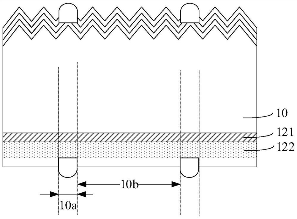
[0024] refer to figure 1 , taking the solar cell as a TOPCon cell as an example.
[0025] In existing applications, the solar cell can be divided into a first region 10a and a second region 10b, the field passivation layer 122 is uniformly covered on the surface of the tunneling layer 121 as a film layer with the same material properties and uniform thickness, and the first region 10a A field passivation layer is used to contact the second electrode.
[0026] The field passivation layer 122 is generally a doped polysilicon layer or an amorphous silicon layer. In order to achieve a saturation recombination current density as low as possible in the second electrode coverage area, that is, the first region 10a, the field passivation layer 122 needs to be heavily Doping to form a relatively obvious energy band bending on the surface of the substrate 10, realize field passivation for minority carriers, realize selective transmission for majority carriers, and form a good ohmic con...
PUM
| Property | Measurement | Unit |
|---|---|---|
| thickness | aaaaa | aaaaa |
| thickness | aaaaa | aaaaa |
| thickness | aaaaa | aaaaa |
Abstract
Description
Claims
Application Information
 - R&D Engineer
- R&D Manager
- IP Professional
- Industry Leading Data Capabilities
- Powerful AI technology
- Patent DNA Extraction
Browse by: Latest US Patents, China's latest patents, Technical Efficacy Thesaurus, Application Domain, Technology Topic, Popular Technical Reports.
© 2024 PatSnap. All rights reserved.Legal|Privacy policy|Modern Slavery Act Transparency Statement|Sitemap|About US| Contact US: help@patsnap.com


