
Grid line structure, solar cell, imbrication assembly, printing method and manufacturing method

A solar cell, solar cell technology, applied in electrical components, final product manufacturing, sustainable manufacturing/processing, etc., can solve difficult second-layer gridlines and dotted gridlines, alignment, second-layer gridlines The extension direction and the extension direction deviate from each other to achieve the effect of improving the processing accuracy and processing efficiency

Pending Publication Date: 2020-03-17
TONGWEI SOLAR ENERGY MEISHAN CO LTD
View PDF0 Cites 2 Cited by
  • Summary
  • Abstract
  • Description
  • Claims
  • Application Information

AI Technical Summary

Problems solved by technology

However, all current screen printing graphic designs of front silver electrodes use straight lines, and the grid lines formed are linear structures that are in full contact with the silicon wafer. The carrier recombination caused by the contact between the grid lines and the silicon wafer limits the battery capacity. Improvement of conversion efficiency
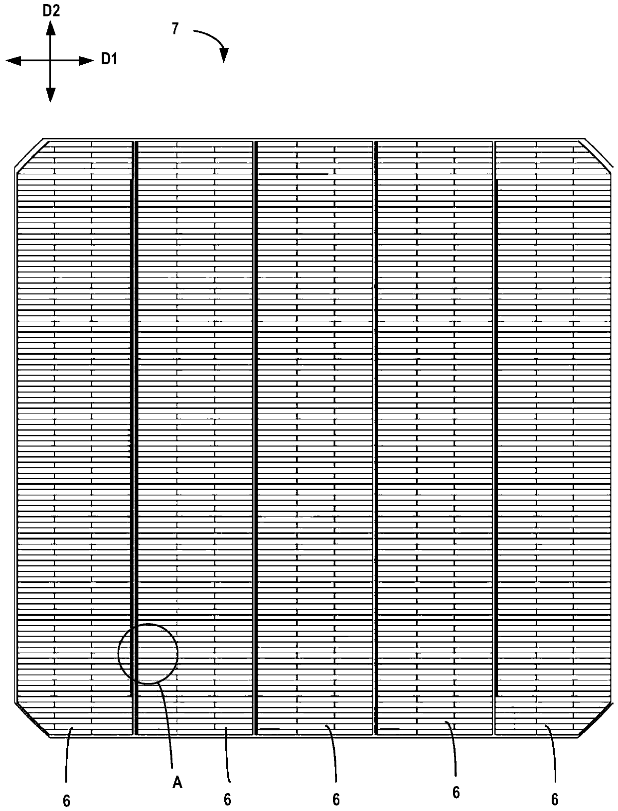
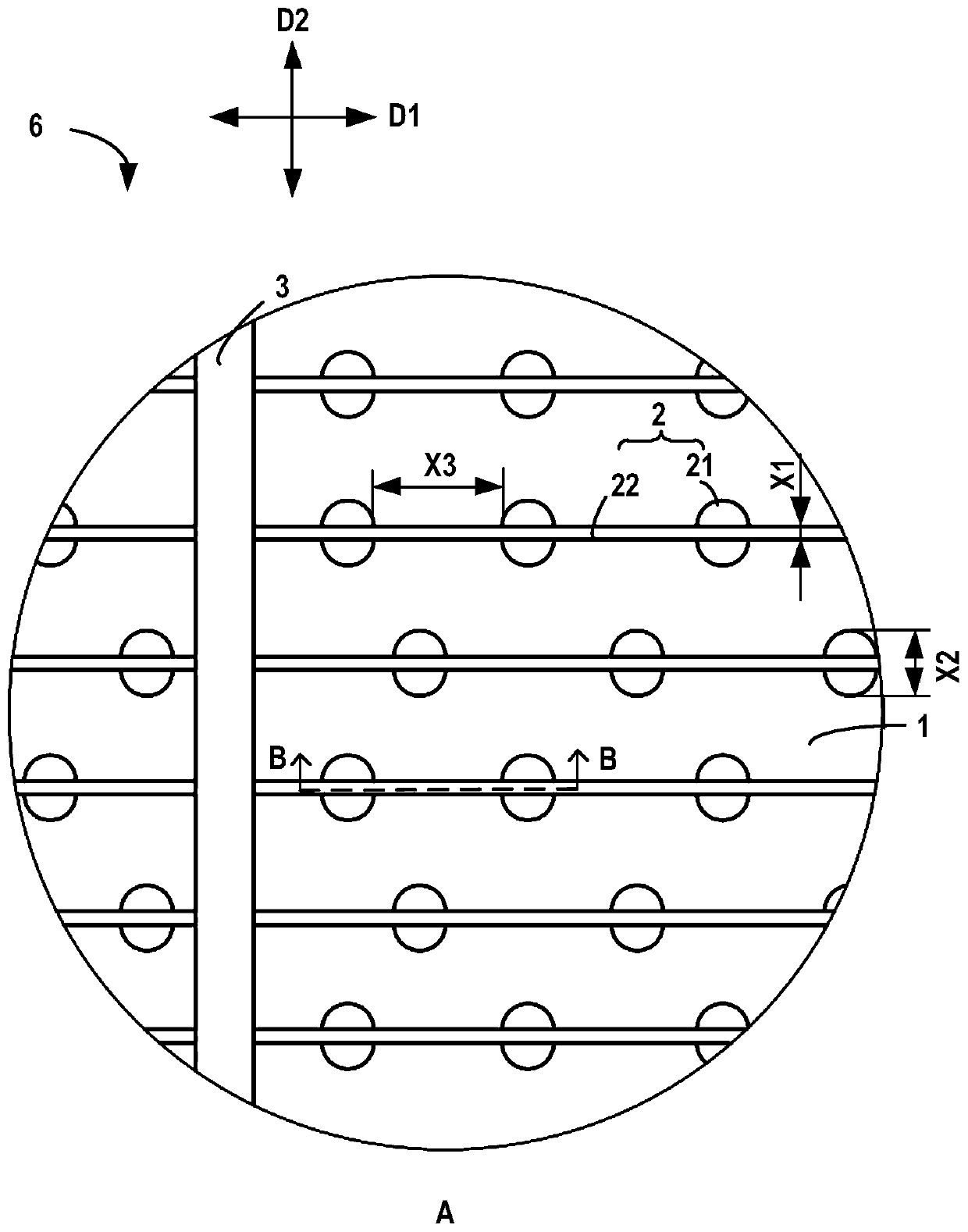
[0007] In order to solve this problem, a layer of dotted grid lines can be set first when setting the grid lines, and then a second layer of grid lines can be set on the dotted grid lines, but there is still a problem in this process: setting the second layer of grid lines It is difficult to align the second-layer grid lines with the dotted-line grid lines, which may cause the extension direction of the second-layer grid lines to deviate from the extension direction of the dotted-line grid lines.

Method used


Image

  • Grid line structure, solar cell, imbrication assembly, printing method and manufacturing method
  • Grid line structure, solar cell, imbrication assembly, printing method and manufacturing method
  • Grid line structure, solar cell, imbrication assembly, printing method and manufacturing method

Examples


Embodiment Construction

[0058] Referring now to the accompanying drawings, specific embodiments of the present invention will be described in detail. What is described here is only a preferred embodiment of the present invention, and those skilled in the art can think of other ways to realize the present invention on the basis of the preferred embodiments, and the other ways also fall within the scope of the present invention.

[0059] The fabrication of crystalline silicon cells requires multiple steps. For monocrystalline silicon cells, it can be obtained as follows. For example, a Czochralski method is used to grow a wafer rod as a raw material. The wafer bar is squared and polished by a square cutting machine to obtain a square bar, and then the square bar obtained after square cutting and grinding is sliced ​​to obtain a single crystal silicon wafer. Afterwards, steps such as surface texturing, cleaning, diffusion junction, removal of phospho-silicate glass, deposition of anti-reflection film ...


PUM

PropertyMeasurementUnit
Widthaaaaaaaaaa
Widthaaaaaaaaaa
Width sizeaaaaaaaaaa

Abstract

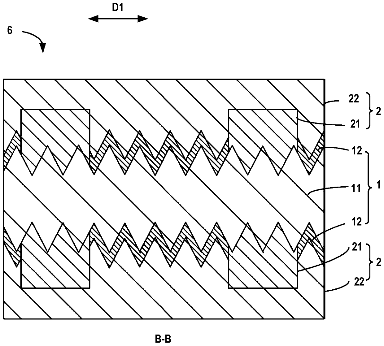
The invention relates to a grid line structure, a solar cell, an imbrication assembly, a printing method and a manufacturing method. The grid line structure is positioned on the top surface and / or thebottom surface of a matrix sheet and comprises a first layer of grid lines and a second layer of grid lines, the first layer of grid lines is in direct contact with a silicon wafer of the matrix sheet, and the second layer of grid lines is arranged at the side, opposite to the matrix sheet, of the first layer of grid lines and is in contact with a film on the silicon wafer. Each first layer of grid line of the two-layer type grid lines comprises a plurality of point-shaped structures, the point-shaped structures are arranged at intervals in the extending direction of the two-layer type grid lines, and the width of the point-shaped structures is larger than that of the second layer of grid lines. According to the invention, the first layer of grid lines is of a dot-shaped structure and thewidth of the first layer of grid lines is greater than that of the second layer of grid lines, so that the second layer of grid lines can be conveniently aligned at the first layer of grid lines during production and manufacture on the basis of reducing the compound of the grid lines and the silicon wafer due to the contact, and the processing precision and the processing efficiency are improved.

Description

technical field [0001] The invention relates to the field of energy, in particular to a grid line structure and a printing method of a crystalline silicon solar cell, a solar cell sheet, a shingled component and a manufacturing method. Background technique [0002] With the accelerated consumption of conventional fossil energy such as coal, oil, and natural gas around the world, and the continuous deterioration of the ecological environment, especially the increasingly severe global climate change caused by greenhouse gas emissions, the sustainable development of human society has been seriously threatened. Countries around the world have formulated their own energy development strategies to deal with the limitation of conventional fossil energy resources and the environmental problems brought about by their development and utilization. Solar energy has become one of the most important renewable energy sources due to its reliability, safety, extensiveness, longevity, environ...

Claims


Application Information

Patent Timeline
IPC IPC(8): H01L31/0224H01L31/18
CPCH01L31/022425H01L31/1804Y02E10/547Y02P70/50
Inventor 常青姚骞张家峰马列王秀鹏
Owner TONGWEI SOLAR ENERGY MEISHAN CO LTD
Learn More