Composite film sensitive material, infrared detector and preparation method
A composite thin film and sensitive material technology, which is applied in semiconductor devices, final product manufacturing, sustainable manufacturing/processing, etc., can solve the problems of low absorption efficiency and low unit photocurrent, and achieve improved photocurrent, enhanced photoresponsivity, Enhance the effect of absorption
- Summary
- Abstract
- Description
- Claims
- Application Information
AI Technical Summary
Problems solved by technology
Method used
Image
Examples
preparation example Construction
[0049] The present invention also provides a method for preparing the composite thin film sensitive material or the composite thin film sensitive material with a carrier, comprising the following steps: sputtering metal on the two-dimensional material; Sputtering metal on the two-dimensional material fixed on the carrier prepared by mechanical peeling and annealing process or prepared by vapor phase deposition method is sufficient.
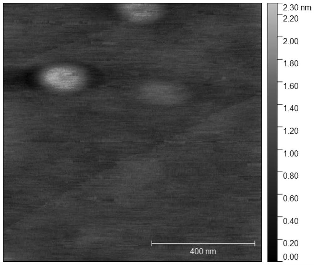
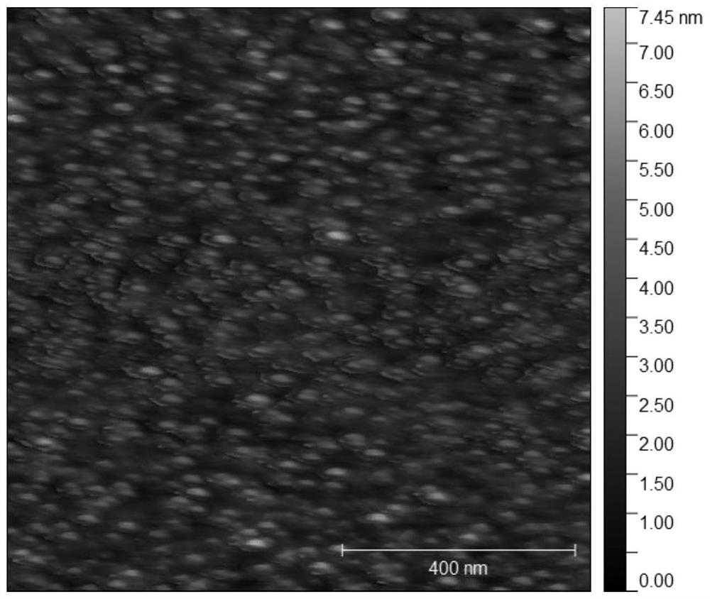
[0050] In the preparation method of the present invention, the sputtering method is a conventional method in the art. However, it has been found by the inventors that if the metal nanoparticles are conical, the diameter of the bottom surface is 5-40 nm, the height is 3-17 nm, and the metal nano-particle layer is a metal nano-particle layer with a single-layer metal nano-particle layer. Control appropriate sputtering conditions, such as sputtering current, vacuum degree, sputtering distance, sputtering speed, sputtering time, etc. These parameters ...
Embodiment 1
[0058] size: figure 1 It is a schematic diagram of a detector, including a silicon dioxide substrate material on the surface, wherein the silicon dioxide thickness is 300nm. A few-layer molybdenum disulfide two-dimensional material obtained by mechanical exfoliation on a silicon dioxide substrate has a size of about 150 μm and a thickness of 3 to 5 layers. The ion sputtering area on the molybdenum disulfide is 50 μm×100 μm and the height is 3 to 12 nm. The gold nanoparticle belt layer, the two ends of the gold nanoparticle belt layer are used as metal electrodes by ion sputtering a 20nm thick titanium layer and an 80nm thick gold layer, and the distance between the left and right source and drain electrodes is 70nm.
[0059] Preparation of molybdenum disulfide layer: The molybdenum disulfide in this example is obtained by mechanical exfoliation method to obtain molybdenum disulfide with few layers of 2H phase, and directly transferred to the silicon dioxide substrate, and then...
PUM
| Property | Measurement | Unit |
|---|---|---|
| diameter | aaaaa | aaaaa |
| height | aaaaa | aaaaa |
| thickness | aaaaa | aaaaa |
Abstract
Description
Claims
Application Information
 - R&D Engineer
- R&D Manager
- IP Professional
- Industry Leading Data Capabilities
- Powerful AI technology
- Patent DNA Extraction
Browse by: Latest US Patents, China's latest patents, Technical Efficacy Thesaurus, Application Domain, Technology Topic, Popular Technical Reports.
© 2024 PatSnap. All rights reserved.Legal|Privacy policy|Modern Slavery Act Transparency Statement|Sitemap|About US| Contact US: help@patsnap.com


