Polarization beam splitter with asymmetric three-waveguide structure and preparation method of polarization beam splitter
A polarization beam splitter and waveguide technology, applied in the field of optical communication, can solve the problems of sensitive bandwidth limitation and large size, and achieve the effect of small size, large working bandwidth and increased working bandwidth
- Summary
- Abstract
- Description
- Claims
- Application Information
AI Technical Summary
Problems solved by technology
Method used
Image
Examples
Embodiment Construction
[0038] In order to make the object, technical solution and advantages of the present invention clearer, the present invention will be further described in detail below in conjunction with specific embodiments and with reference to the accompanying drawings.
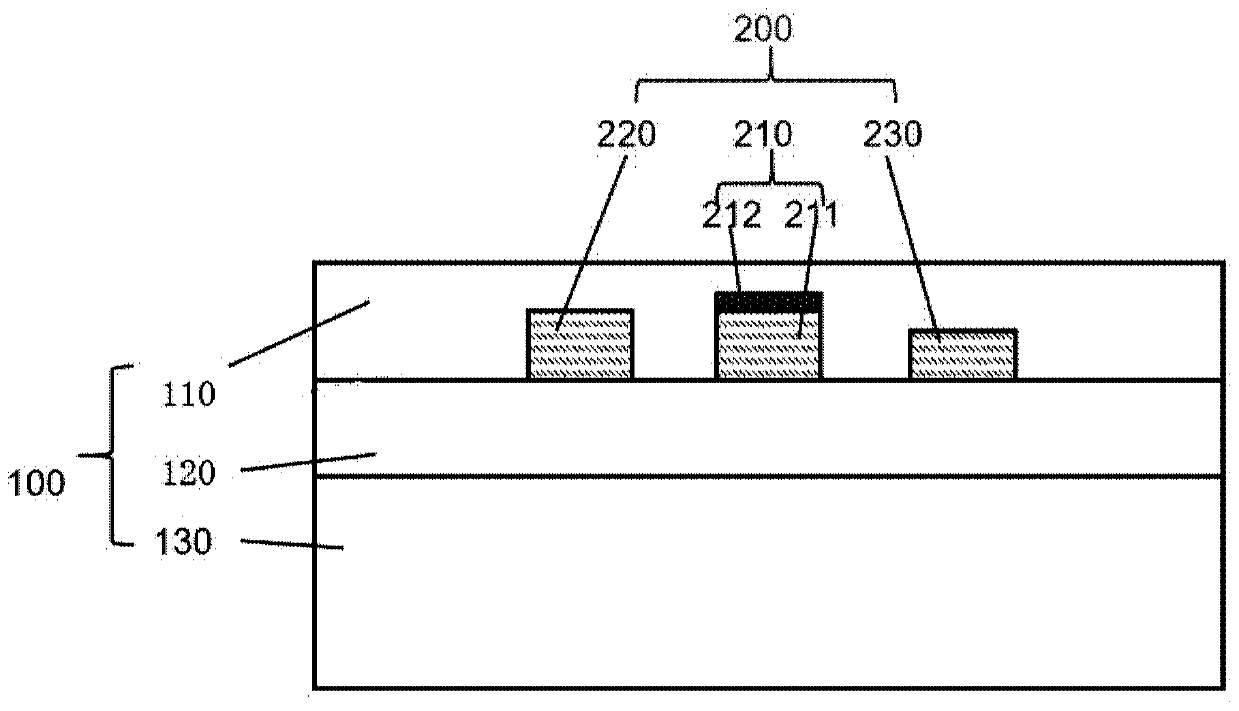
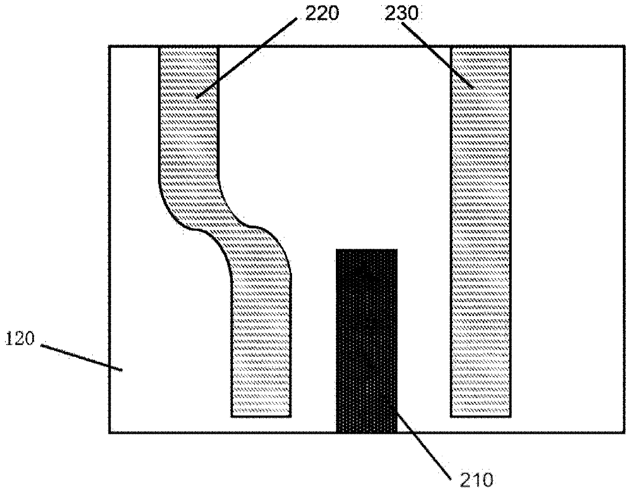
[0039] see figure 1 and figure 2 As shown, the present invention provides a polarization beam splitter with an asymmetric three-waveguide structure, including: SO1 substrate layer 100 and waveguide layer 200, wherein,
[0040] SOI substrate layer 100, comprising a bottom Si material layer 130, a silicon dioxide buried layer 120 formed above the bottom Si material layer, and a cladding layer 110 covering above the waveguide layer;
[0041] The waveguide layer 200 is fabricated on the silicon dioxide buried layer 120, including an input waveguide 210, a TM mode coupling waveguide 220, and a TE mode coupling waveguide 230, and the input waveguide 210 includes a bottom waveguide 211 and a dielectric cover layer 212; wherein...
PUM
 Abstract
Description
Claims
Application Information
 - R&D
- Intellectual Property
- Life Sciences
- Materials
- Tech Scout
- Unparalleled Data Quality
- Higher Quality Content
- 60% Fewer Hallucinations
Browse by: Latest US Patents, China's latest patents, Technical Efficacy Thesaurus, Application Domain, Technology Topic, Popular Technical Reports.
© 2025 PatSnap. All rights reserved.Legal|Privacy policy|Modern Slavery Act Transparency Statement|Sitemap|About US| Contact US: help@patsnap.com


