Resistive random access memory and preparation method thereof
A resistive variable memory and resistive variable technology, applied in the field of memory, can solve the problems of reducing the reliability of stored data, misreading and miswriting of stored information, etc.
- Summary
- Abstract
- Description
- Claims
- Application Information
AI Technical Summary
Problems solved by technology
Method used
Image
Examples
preparation example Construction
[0023] The invention provides a method for preparing a resistive variable memory, comprising the following steps:
[0024] Depositing a resistive switch material on the bottom electrode to form an amorphous resistive switch layer;
[0025] preparing a nanotube array on the amorphous resistive layer to form a shielding layer;
[0026] Perform oxygen plasma enhanced annealing treatment on the overall structure forming the shielding layer to convert the amorphous resistive layer into a highly crystalline array region;
[0027] The shielding layer is removed, and a top electrode is prepared on the surface of the highly crystalline array region to obtain a resistive variable memory.
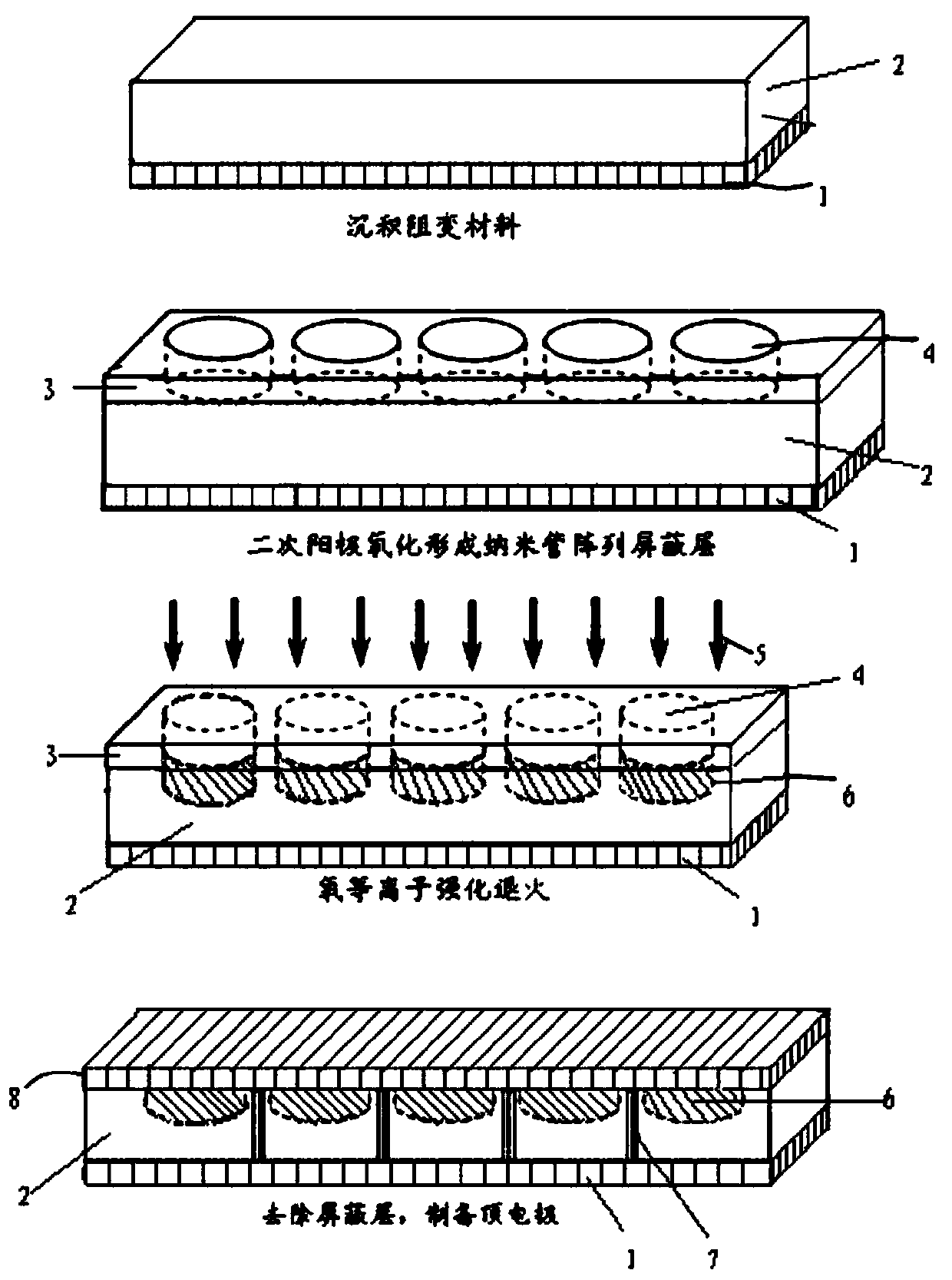
[0028] In order to clearly illustrate the solution of the present invention, the following specific embodiments refer to figure 1 The schematic diagram of the process shown in the illustration:
[0029] In the present invention, a resistive switch material is deposited on the bottom electrode 1 to ...
Embodiment 1
[0047] according to figure 1 The flow schematic diagram shown in the preparation of resistive memory, the specific steps are as follows:
[0048] Prepare the Cr / Cu / Cr metal film system on the surface of the silicon substrate by DC sputtering method as the bottom electrode of the resistive variable memory; when depositing, control the deposition process parameters as follows: the chromium target is used as the sputtering target, and the substrate temperature does not exceed 100°C (Control at 90°C, the substrate temperature of the following steps is the same), sputtering power 100W, sputtering time 3min and copper target as sputtering target, substrate temperature below 100°C, sputtering power 100W, sputtering time 2min; After deposition, a Cr / Cu / Cr bottom electrode is obtained, wherein the thickness of the single-layer Cr is 10nm, and the thickness of Cu is 10nm;
[0049] Continue to prepare a layer of TiO with a thickness of about 100nm by radio frequency magnetron sputtering...
Embodiment 2~3
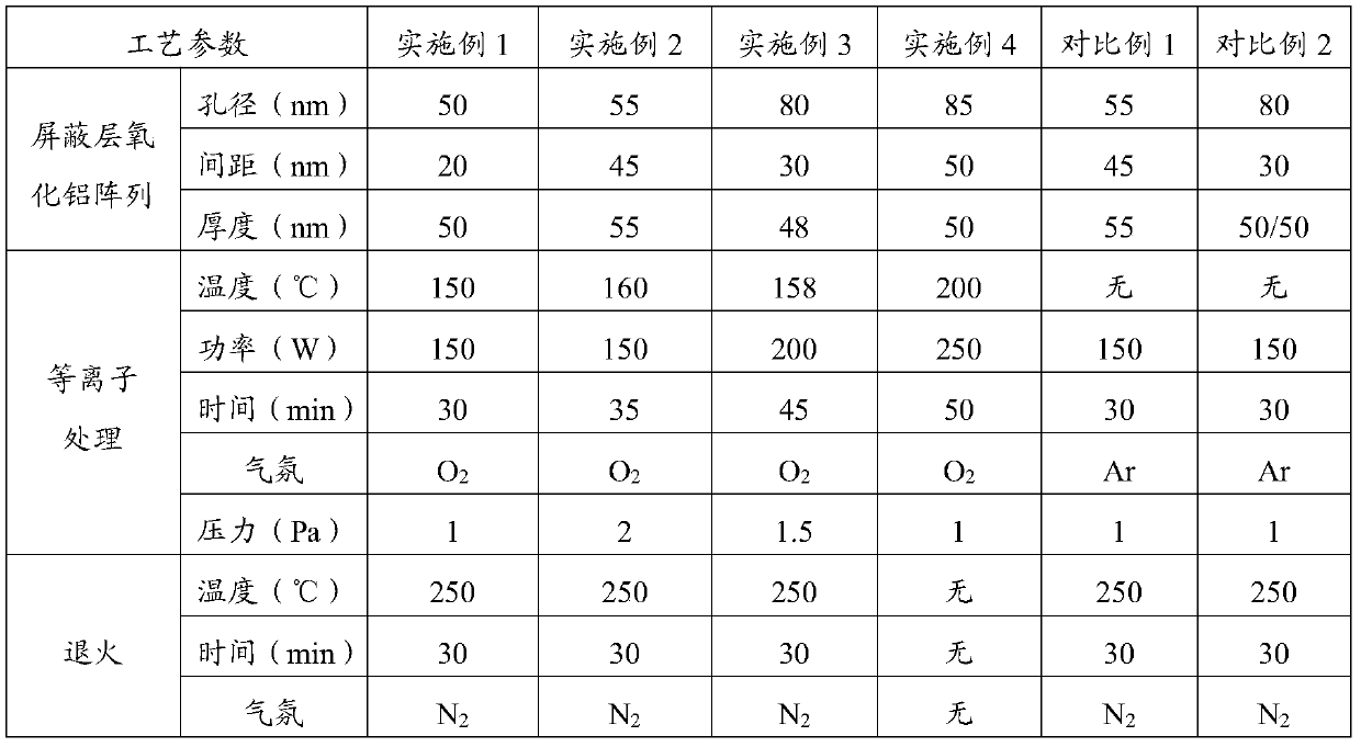
[0059] The RRAM was prepared according to the method of Example 1, except that the thickness of each deposited material layer and the annealing process parameters were different, which are specifically listed in Table 1.
PUM
| Property | Measurement | Unit |
|---|---|---|
| thickness | aaaaa | aaaaa |
| diameter | aaaaa | aaaaa |
| depth | aaaaa | aaaaa |
Abstract
Description
Claims
Application Information
 - Generate Ideas
- Intellectual Property
- Life Sciences
- Materials
- Tech Scout
- Unparalleled Data Quality
- Higher Quality Content
- 60% Fewer Hallucinations
Browse by: Latest US Patents, China's latest patents, Technical Efficacy Thesaurus, Application Domain, Technology Topic, Popular Technical Reports.
© 2025 PatSnap. All rights reserved.Legal|Privacy policy|Modern Slavery Act Transparency Statement|Sitemap|About US| Contact US: help@patsnap.com


