Semiconductor Structure with Material Modification and Low Resistance Plug

A manufacturing method and technology of integrated circuits, applied in the manufacturing of circuits, electrical components, semiconductor/solid-state devices, etc., can solve problems such as voids or other defects, and inability to fully meet requirements

Inactive Publication Date: 2020-01-07
TAIWAN SEMICON MFG CO LTD
View PDF0 Cites 0 Cited by
  • Summary
  • Abstract
  • Description
  • Claims
  • Application Information

AI Technical Summary

Problems solved by technology

Also, filling the contact holes with metal is another challenge or consideration that can create voids or other defects
[0004] Existing FinFET devices are therefore generally suitable for their development purposes, but not in all respects

Method used


Image

  • Semiconductor Structure with Material Modification and Low Resistance Plug
  • Semiconductor Structure with Material Modification and Low Resistance Plug
  • Semiconductor Structure with Material Modification and Low Resistance Plug

Examples


Embodiment Construction

[0057] Different embodiments or examples provided below may implement different configurations of the present invention. The examples of specific components and arrangements are used to simplify the invention and not to limit the invention. For example, the statement that a first component is formed on a second component includes that the two are in direct or physical contact, or there are other additional components interposed therebetween rather than in direct contact. In addition, numbers may be repeated in various examples of the present disclosure, but these repetitions are only for simplification and clarity of illustration, and do not mean that units with the same numbers in different embodiments and / or arrangements have the same corresponding relationship.

[0058] In addition, spatial relative terms such as "below", "beneath", "lower", "above", "above", or similar terms may be used to simplify describing the relationship between one element and another element in the ...


PUM


Abstract

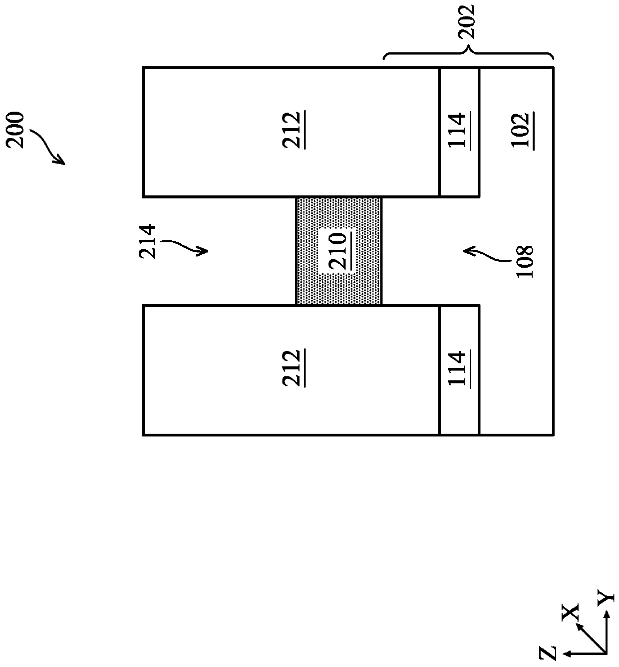
The present disclosure provides a method of fabricating an integrated circuit (IC) structure. The method includes the steps: patterning a dielectric layer on a semiconductor substrate to form a trench, exposing a conductive feature within the trench; performing an ion implantation process to introduce a doping species into sidewalls of the dielectric layer within the trench, thereby forming a barrier layer on the sidewalls, the barrier layer having a densified structure to effectively prevent inter-diffusion and a modified surface characteristic to boost a bottom-up deposition; and performingthe bottom-up deposition to fill the trench with a metal material, thereby forming a metal plug landing on the conductive feature.

Description

technical field [0001] Embodiments of the present invention relate to a method for forming a semiconductor device, and more particularly to a method for forming a metal plug. Background technique [0002] The semiconductor industry has progressed to nanotechnology process nodes for higher device density, higher performance, and lower cost. Along with the above progress, fabrication and design challenges lead to the development of three-dimensional designs, such as FinFET devices. A typical FinFET device is fabricated by extending thin fins or fin structures from a substrate. The fins typically comprise silicon and form the body of the transistor device. The channels of the transistors are formed in this vertical fin. The gate is on the fin (eg wrapping the fin). This form of gate has greater control over the channel. Other advantages of FinFET devices include reduced short channel effects and increased current flow. [0003] However, existing FinFET device structures s...

Claims


Application Information

Patent Timeline
IPC IPC(8): H01L21/768H01L29/78
CPCH01L21/76897H01L29/785
Inventor 莫如娜·阿比里杰斯·柯德博峰地辉
Owner TAIWAN SEMICON MFG CO LTD
Why Eureka
Try Eureka