
A kind of preparation technology of flexible transparent conductive film

A technology of transparent conductive film and preparation process, which is applied to equipment for manufacturing conductive/semiconductive layers, cable/conductor manufacturing, circuits, etc., can solve the problems of large resistance value of conductive film, complex lithography technology and high cost

Active Publication Date: 2021-02-02
厦门派恩杰科技有限公司
View PDF8 Cites 0 Cited by
  • Summary
  • Abstract
  • Description
  • Claims
  • Application Information

AI Technical Summary

Problems solved by technology

The existence of a large number of bonding points between metal nanowires makes the resistance of the conductive film larger, which limits its further application in the field of flexible electronics
At present, most metal nanogrids are prepared by photolithography technology and coating technology. The photolithography technology is complex and costly, which is not conducive to large-area roll-to-roll production.

Method used


Image

  • A kind of preparation technology of flexible transparent conductive film
  • A kind of preparation technology of flexible transparent conductive film
  • A kind of preparation technology of flexible transparent conductive film

Examples


preparation example Construction

[0029] The invention provides a preparation process of a flexible transparent conductive film, and the specific steps of the preparation process include:

[0030] (1) Colloidal solution is evenly coated on the substrate to form a colloidal layer;

[0031] (2) cutting the colloidal layer to form a grid morphology;

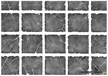
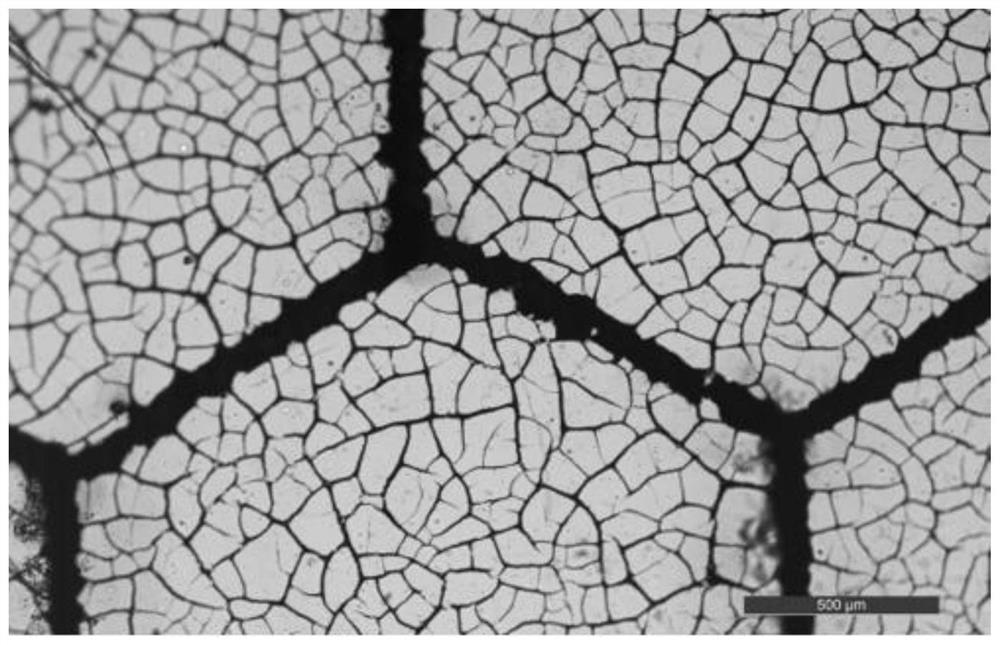
[0032] (3) drying the colloidal layer after cutting to make it dry and crack to produce micron-scale crack templates;

[0033] (4) depositing metal on the colloidal layer gained in step (3);

[0034] (5) removing the colloid from the film obtained in step (4) to obtain a flexible transparent conductive film;

[0035] Specifically, in step (2), the depth of cutting the colloidal layer is equal to the thickness of the coated colloidal layer, through the design of the cutting depth equal to the thickness of the colloidal layer, the purpose of cutting through the colloidal layer is realized, so as to realize the subsequent metal deposition process , the metal deposit...

Embodiment 1

[0049] The first embodiment of the present invention provides a preparation process of a flexible transparent conductive film, and the specific steps of the preparation process include:

[0050] (1) Cut a polyethylene terephthalate (PET) film (light transmittance ~ 95%) with a thickness of 100 μm into a rectangular piece of 50cm*60cm, wash it with deionized water and absolute ethanol for 30min, respectively, Dry and use as a base. Prepare TiO with a concentration of 5% 2 weak. TiO with a thickness of 1 μm was sprayed 2 The colloidal solution is evenly applied to the surface of the PET substrate;

[0051] (2) The grid is processed on the colloidal layer by laser cutting colloidal film technology, and the shape of the grid is controlled by computer to be a triangular grid. The processing line spacing is 700 μm, the line width is 100 μm, and the cutting speed of the laser cutting machine is 80mm / s;

[0052] (3) Place the cut colloid film at an air pressure of 1*10 -3 Pa, dry...

Embodiment 2

[0056] The steps of the second embodiment are roughly the same as those of the first embodiment. The difference is that in this embodiment, in step (2), the grid is processed on the colloidal layer by laser cutting colloidal film technology, and the grid shape is a rectangular grid. .

[0057] Embodiment 2 of the present invention provides the same implementation principles and technical effects as Embodiment 1. For brief description, for details not mentioned in this embodiment, reference may be made to the corresponding content in Embodiment 1.


PUM


Abstract

The invention provides a preparation process of a flexible transparent conductive film, which relates to the technical field of electronic devices; the invention first cuts through the colloidal layer on the colloidal layer according to the grid shapes of triangles, rectangles and hexagons through laser cutting colloidal film technology After the mesoscale cracks are obtained, the colloidal solution on the substrate dries up to produce microscale cracks. On the colloid layer that has produced microscale and mesoscale cracks, the metal is deposited on the microscale and mesoscale by magnetron sputtering technology. In the crack, and remove the colloid on the substrate, and finally obtain the conductive film of the substrate and the composite metal mesh covered on the substrate; the prepared conductive film has excellent conductivity, and can realize its resistance value after repeated bending Almost unchanged, its production process is non-toxic and harmless, low in cost, easy to operate, and can be mass-produced. The flexible transparent conductive film produced can replace the traditional ITO conductive film and is used in light-emitting electronic devices, touch screen panels, etc. field of electronic devices.

Description

technical field [0001] The invention relates to the field of electronic device manufacturing, in particular to a preparation process of a flexible transparent conductive film. Background technique [0002] Transparent conductive electrodes with excellent mechanical flexibility will become an important component of next-generation wearable optoelectronic devices, occupying an increasingly important position in the fields of light-emitting devices, photovoltaic cells, touch screen panels, etc. Tin-doped indium oxide (ITO) has become the most widely used transparent conductive film material in academia and industry due to its optical transparency, thermal and chemical stability, device compatibility, and well-developed fabrication process. [0003] Although the preparation of ITO plastic films has been achieved, its application in various wearable optoelectronic devices is still limited due to the brittle nature of ITO. In addition, the high cost of indium element also makes t...

Claims


Application Information

Patent Timeline
Patent Type & Authority Patents(China)
IPC IPC(8): H01B13/00
CPCH01B13/00H01B13/0026
Inventor 许清池苏秋聪王金贵郭季丰
Owner 厦门派恩杰科技有限公司
Learn More