Array substrate and manufacturing method

A technology of an array substrate and a manufacturing method, which is applied in the field of liquid crystal display panels, can solve problems such as increased parasitic capacitance, abnormal splash screen, wrong writing of signals, etc., and achieves reduction of area, improvement of aperture ratio, and constant resistance of resistance. Effect

Active Publication Date: 2020-08-28
TCL CHINA STAR OPTOELECTRONICS TECH CO LTD
View PDF8 Cites 0 Cited by
  • Summary
  • Abstract
  • Description
  • Claims
  • Application Information

AI Technical Summary

Problems solved by technology

[0003] Thin Film Transistor (TFT) liquid crystal display is the most common liquid crystal display in the mainstream market at present, and the TFT pixel design generally adopts a light-shielding structure design to reduce the problem of excessive leakage current caused by backlight illumination; the light-shielding structure One of the major disadvantages is that there will be a large parasitic capacitance, resulting in a large Feedthrough (vacuum) voltage, resulting in incorrect signal writing
At present, large-size panels require the line width of the scanning lines to be as large as possible to drive the panel normally, but this will increase the parasitic capacitance of the data lines and scanning lines, resulting in RC delay (RC Delay, that is, the increase in capacitance and resistance causes delay Time), which will cause abnormal Flicker

Method used


Image

  • Array substrate and manufacturing method
  • Array substrate and manufacturing method
  • Array substrate and manufacturing method

Examples


Embodiment Construction

[0034] The present invention will be described in further detail below in conjunction with the accompanying drawings and embodiments.

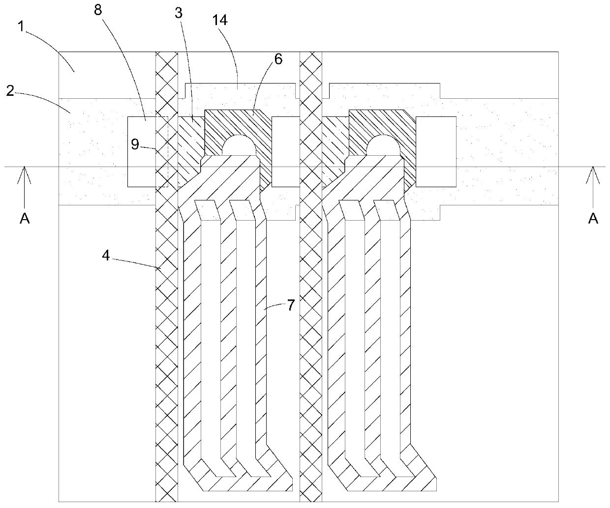
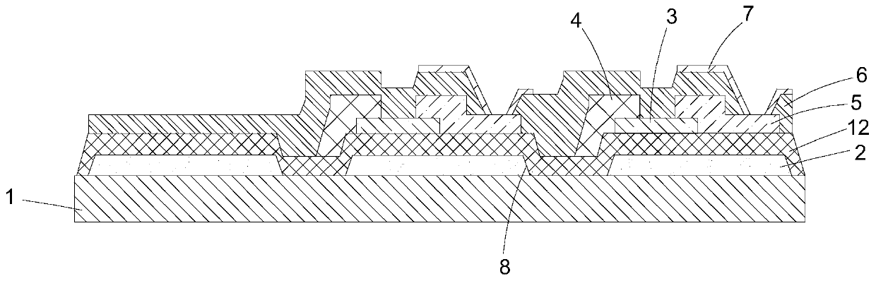
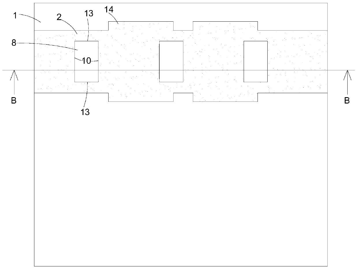
[0035] exist Picture 1-1 , 2-1 , 3-1, 4-1, and 5-1 only show the positional relationship of devices related to the present invention.

[0036] Such as Picture 1-1 and Figure 1-2 As shown, an array substrate of the present invention includes a substrate 1, a plurality of scanning lines (gate lines) 2, an active layer 3 arranged on the scanning lines 2, and a plurality of data lines interlaced with the scanning lines 2 4. The drain electrode 5 in contact with the active layer 3, the passivation layer 6 formed on the drain electrode 5, and the pixel electrode 7 formed on the passivation layer 6; between the scanning line 2 and the active layer 3, a Layer gate insulating layer 12, the pixel electrode 7 is connected to the drain electrode 5 through the via hole on the passivation layer 6; scanning line holes 8 are respectively opened at the po...


PUM


Abstract

The invention provides an array substrate comprising a substrate, a plurality of scanning lines, an active layer arranged on the scanning lines, a plurality of data lines interlaced with the scanning lines, a drain electrode contacted with the active layer, a passivation layer formed on the drain electrode and a pixel electrode formed on the passivation layer, wherein a scanning line hole is formed in positions, where the data lines are interlaced, on the scanning lines respectively; and in the lines interlaced with the scanning lines on the data lines, part of the lines are overlapped with the scanning line holes, and the other part of the lines are overlapped with the active layer and in overlapping joint with one another. The invention further provides a manufacturing method of the array substrate. Compared with the prior art, by forming the scanning line holes in the positions where the data lines are interlaced on the scanning lines, the overlapping area between the scanning lines and the data lines is reduced, then the parasitic capacitance is reduced and the influence of a vacuum voltage on panel display is reduced, so that the resistance value of the electric resistance of the scanning lines can keep unchanged while the aperture opening rate of a pixel electrode is improved.

Description

technical field [0001] The invention relates to a liquid crystal display panel technology, in particular to an array substrate and a manufacturing method. Background technique [0002] Liquid Crystal Display (LCD) has many advantages such as thin body, power saving, and no radiation, and has been widely used, such as: LCD TV, mobile phone, personal digital assistant (PDA), digital camera, computer screen or Laptop screens, etc., dominate the field of flat panel displays. [0003] Thin Film Transistor (TFT) liquid crystal display is the most common liquid crystal display in the mainstream market at present, and the TFT pixel design generally adopts a light-shielding structure design to reduce the problem of excessive leakage current caused by backlight illumination; the light-shielding structure One of the major drawbacks is the large parasitic capacitance, resulting in a large Feedthrough (vacuum) voltage, resulting in wrong writing of signals. At present, large-size panel...

Claims


Application Information

Patent Timeline
Patent Type & Authority Patents(China)
IPC IPC(8): G02F1/1362
CPCG02F1/136227G02F1/136286
Inventor 林碧芬甘启明
Owner TCL CHINA STAR OPTOELECTRONICS TECH CO LTD
Why Eureka
Try Eureka