
Patsnap Eureka
For R&D, Patsnap Eureka makes reading and utilizing patents & technical documents easy.
Patsnap Eureka AIR
Designed for self-driven R&D workflows. Generate viable solutions, solve complex R&D challenges, empower your innovation with AI.

Patsnap Eureka Materials
Designed for material experts only. Revolutionize your material R&D, from search, analyze, to developing new materials.

TechResearch
Generate reliable direction feasibility study reports for your R&D in just a few steps.

TechSeek
Discover and master advanced knowledge NOW. Basics, ideas, possibilities, all at once.

TechMind
As an expert in R&D Theories, TechMind can generates customized viable solutions instantly.

TechRisk
Analyze your overall solution with one click, know your potential R&D risks in advance.

TechMonitor
Get weekly tech updates, stay abreast of the latest tech innovations and key insights.
Flexible transparent conductive film and preparation technology thereof
A technology of transparent conductive film and preparation process, which is applied in the direction of equipment for manufacturing conductive/semiconductive layers, cable/conductor manufacturing, conductive layers on insulating carriers, etc., and can solve the limitations of the application in the field of flexible electronics and the complexity of photolithography technology , high resistance of the conductive film, etc.
- Summary
- Abstract
- Description
- Claims
- Application Information
AI Technical Summary
Problems solved by technology
Method used
Image

Examples
Embodiment 1
[0059] The first embodiment of the present invention provides a preparation process of a flexible transparent conductive film, and the specific steps of the preparation process include:
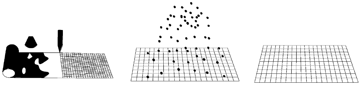
[0060] (1) Cut a polyethylene terephthalate (PET) film (light transmittance ~ 95%) with a thickness of 100 μm into a rectangular piece of 50cm*60cm, wash it with deionized water and absolute ethanol for 30min, respectively, Dry and use as a base. Prepare TiO with a concentration of 5% 2 weak. TiO with a thickness of 1 μm was sprayed 2 The colloidal layer is evenly coated on the surface of the PET substrate;
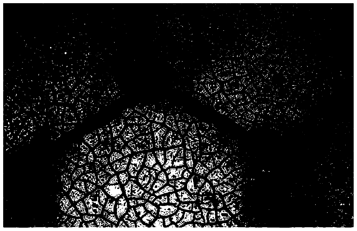
[0061] (2) Place the colloidal film in step (1) at an air pressure of 1*10 -3 Pa, the humidity is 40%, and the temperature is 55°C and dried to make it evenly cracked;
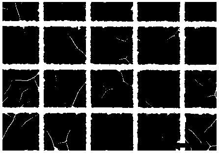
[0062] (3) Then the grid is processed on the colloidal template by laser cutting colloidal film technology, and the shape of the grid is controlled by the computer as a triangular grid such as Figure 4 As shown in...
Embodiment 2
[0066] The steps of the second embodiment are roughly the same as those of the first embodiment. The difference is that in this embodiment, in step (3), the grid is processed on the colloidal template by laser cutting colloidal film technology, and the grid shape is a rectangular network. grid, such as Figure 4 (b) shown.
[0067] Embodiment 2 of the present invention provides the same implementation principles and technical effects as Embodiment 1. For brief description, for details not mentioned in this embodiment, reference may be made to the corresponding content in Embodiment 1.
Embodiment 3
[0069] The steps of the third embodiment are roughly the same as those of the first embodiment. One of the differences is that in this embodiment, in step (3), the grid is processed on the colloidal template by laser cutting colloidal film technology, and the grid shape is A hexagonal grid such as Figure 4 As shown in (c), the second difference is that in step (5), the film is immersed in absolute ethanol to remove the colloid, and dried to obtain a flexible transparent conductive film.
[0070] Embodiment 3 of the present invention provides the same implementation principles and technical effects as Embodiment 1. For brief description, for details not mentioned in this embodiment, reference may be made to the corresponding content in Embodiment 1.
PUM
| Property | Measurement | Unit |
|---|---|---|
| Length | aaaaa | aaaaa |
| Length | aaaaa | aaaaa |
| Square resistance | aaaaa | aaaaa |
Abstract
Description
Claims
Application Information
 - R&D Engineer
- R&D Manager
- IP Professional
- Industry Leading Data Capabilities
- Powerful AI technology
- Patent DNA Extraction
Browse by: Latest US Patents, China's latest patents, Technical Efficacy Thesaurus, Application Domain, Technology Topic, Popular Technical Reports.
© 2024 PatSnap. All rights reserved.Legal|Privacy policy|Modern Slavery Act Transparency Statement|Sitemap|About US| Contact US: help@patsnap.com