
RFID tag of silver paste antenna process and chip packaging method

An RFID label and chip packaging technology, which is applied to record carriers, instruments, and computer parts used in machines. It can solve the problems of limited selection of label substrates, low packaging qualification rate, substrate deformation, etc., and improve packaging. Productivity and RFID tag throughput, parasitic resistance and capacitance suppression, cost and energy reduction effects

Active Publication Date: 2019-12-13
迈思成(北京)科技有限公司
View PDF3 Cites 1 Cited by
  • Summary
  • Abstract
  • Description
  • Claims
  • Application Information

AI Technical Summary

Problems solved by technology

The method in the prior art has the following defects: (1) Functional defects: Since the chip and the antenna are not in direct contact with each other, but are connected through an anisotropic conductive adhesive to achieve electrical conduction, in the process of hot pressing, due to the connection of the conductive adhesive , will introduce parasitic resistance and parasitic capacitance between the chip and the antenna, resulting in a certain range of deviations in the matching between the chip and the antenna, which will affect multiple technical indicators such as label reading and sensitivity; (2) Functional defects: in the chip packaging During the process, due to the temperature and pressure of the chip and the silver paste antenna for a certain period of time, the chip with a relatively thin thickness (below 800nm) will be broken by pressure, which makes this process unsuitable for packaging ultra-thin RFID chips.
Compared with aluminum etching / copper etching antennas, silver paste antennas are not resistant to high temperature and high pressure. During the chip bonding process, due to excessive pressure or high temperature, the silver paste line at the chip packaging point is broken, forming a dark break. , which in turn leads to poor function or failure of the label, and this kind of fracture is located under the chip, which is difficult to find and detect
At present, the binding temperature of this process in the market is in the range of 135-210 degrees Celsius. Due to the effect of high temperature and high pressure, some label substrates will have indentations at the chip position, and the indentations will generally appear in the shape of a thermal head, which will affect the label. The aesthetics, for the non-temperature-resistant RFID label substrate, the deformation of the substrate due to the high temperature at the packaging position, for low-temperature materials (melting point below 120 degrees Celsius) such as PP, PE, PVC, synthetic materials, carbon film, etc. It is not possible to apply the process
Since a variety of low-temperature materials cannot be applied to RFID tags, this is also the main reason why RFID tags cannot be applied in some special fields
(3) High cost: At present, when this process is used for chip packaging of aluminum etching or copper etching antennas, the packaging qualification rate is about 99.3%, while the silver paste printing antenna is only 97%. This is the parameter of the original imported packaging equipment. The packaging pass rate of domestic equipment will be lower. The low packaging pass rate will lead to an increase in the cost of the label quality inspection process, and the cost of the finished RFID label will also increase.
Due to the high price of glue, it also increases the cost of RFID tags
(4) High energy consumption: During the binding process, the hot pressing temperature is in the range of 135-210 degrees Celsius, and the time will last for 4-10s. High-temperature binding results in high energy consumption
(5) Low efficiency: chip binding has always been the bottleneck of production capacity in the process of RFID label processing. Due to the heat pressure of 4-10s in the chip binding process, the efficiency of the binding equipment cannot be improved. Currently, this method is used in the market. The production capacity of mainstream imported binding equipment in the process is 7000-11000 labels per hour, while the production capacity of domestic equipment is 4000-8000 labels
[0004] Therefore, the shortcomings of the existing RFID silver paste antenna packaging process are mainly the introduction of large values ​​of parasitic resistance and capacitance, antenna breakage and chip breakage, limited selection of label substrates, high energy consumption and low production capacity.

Method used


Image

  • RFID tag of silver paste antenna process and chip packaging method
  • RFID tag of silver paste antenna process and chip packaging method
  • RFID tag of silver paste antenna process and chip packaging method

Examples


Embodiment Construction

[0043] In order to make the objectives, technical solutions, and advantages of the present invention clearer, the present invention will be further described in detail below in conjunction with specific embodiments and with reference to the accompanying drawings. It should be understood that these descriptions are only exemplary and are not intended to limit the scope of the present invention. In addition, in the following description, descriptions of well-known structures and technologies are omitted to avoid unnecessarily obscuring the concept of the present invention.

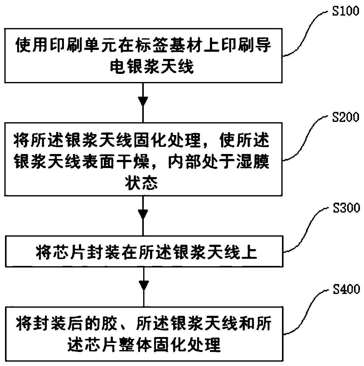
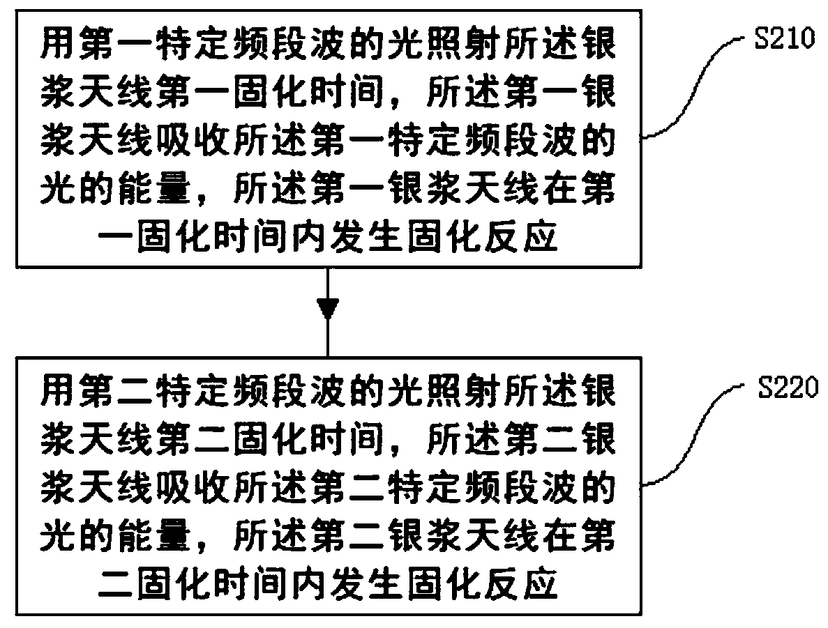
[0044] RFID tags use special conductive silver paste, and use a printer to print the silver paste antenna on the label substrate; the line automatically flows to the curing unit to dry the surface of the silver paste antenna; then enters the packaging equipment for the chip binding process; binding After the end, the line will automatically flow to the secondary overall curing unit for the overall drying and cu...


PUM


Abstract

The invention relates to an RFID (Radio Frequency Identification Device) label of a silver paste antenna process and a chip packaging method, and an RFID label chip comprises a label base material, asilver paste antenna, glue and a chip, the packaging method comprises the following steps: printing a conductive silver paste antenna on a label substrate by using a printing unit; curing the silver paste antenna, so that the surface of the silver paste antenna is dry, and the interior of the silver paste antenna is in a wet film state; packaging a chip on the silver paste antenna; and integrallycuring the packaged silver paste antenna and the packaged chip. The RFID silver paste antenna packaging procedure can be optimized. Chip packaging is simpler, dependence on high-precision equipment isreduced, standardized and process production is achieved. Meanwhile, the packaging percent of pass is increased, cost and energy consumption are reduced. Optimization of the silver paste antenna printing process before packaging is driven, and the packaging capacity and the RFID label capacity are improved.

Description

Technical field [0001] The invention relates to the technical field of semiconductor packaging, in particular to a silver paste antenna technology RFID tag and a chip packaging method. Background technique [0002] With the rapid development of big data technology, cloud technology, 5G technology, and AI technology, RFID, as the basic sensing layer information collection technology of the Internet of Things, has also begun to develop and apply on a large scale in the past 5 years. Since 2017, in the global market, especially represented by China, RFID technology has been widely used in new retail, clothing logistics, store management, logistics management and other fields. At present, almost all domestic unmanned supermarkets use RFID technology. To manage. At the same time, the market demand for RFID tags is increasing year by year, especially for low-price RFID. RFID tags have begun to turn to low value-added commodity applications. Reducing the cost of RFID tags is a decisive...

Claims


Application Information

Patent Timeline
Patent Type & Authority Applications(China)
IPC IPC(8): G06K19/077
CPCG06K19/07745G06K19/0776G06K19/07773
Inventor 冯海波赵海军王启祥李志丹周书娟
Owner 迈思成(北京)科技有限公司
Learn More