Multi-level fused three-dimensional system integrated structure

A system-integrated, multi-level technology, applied in electrical components, electro-solid devices, circuits, etc., can solve the problems of complex and immature process technology, unable to meet the miniaturization, high performance and low power consumption of micro-system products, and achieve The effect of simplifying process method, saving cost and ensuring power integrity

Active Publication Date: 2019-12-06
XIDIAN UNIV
View PDF7 Cites 2 Cited by
  • Summary
  • Abstract
  • Description
  • Claims
  • Application Information

AI Technical Summary

Problems solved by technology

[0004] In view of the above problems, the purpose of the present invention is to solve the complex and immature process technology in the existing three-dimensional system integration structure, which cannot meet the requirements of miniaturization, high performance and low power consumption of microsystem products.

Method used


Image

  • Multi-level fused three-dimensional system integrated structure
  • Multi-level fused three-dimensional system integrated structure

Examples


Embodiment 1

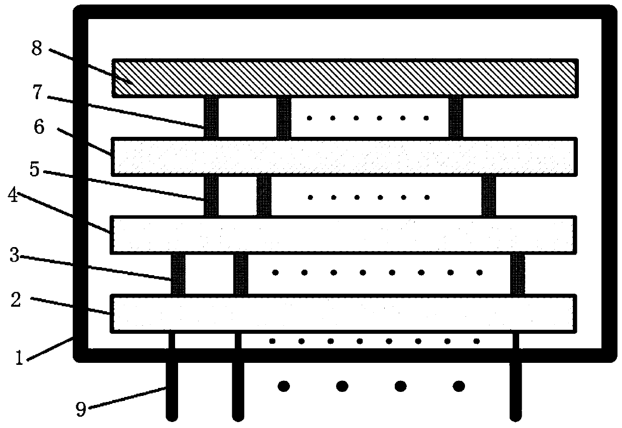
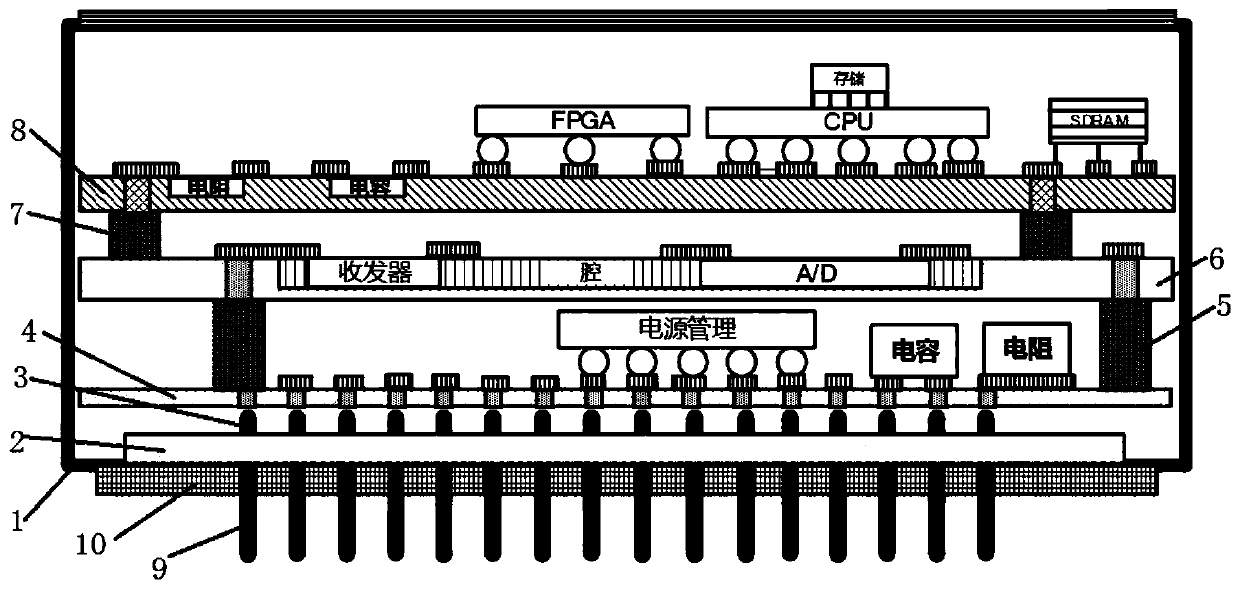
[0021] In order to solve the complex and immature process technology of the existing three-dimensional system integration structure, it cannot meet the requirements of miniaturization, high performance and low power consumption of microsystem products. This embodiment provides a figure 1 The shown multi-level integrated three-dimensional system integration structure includes a shell 1, which is used to protect various chips and devices in the multi-level integrated three-dimensional integrated circuit, providing good airtightness, and facilitating the installation and application of the three-dimensional system integrated structure The bottom surface of the tube shell 1 is provided with a plurality of pins 9, and the tube shell 1 is provided with n sequentially stacked substrate modules, and the n substrate modules are respectively provided with chips and resistance capacitor devices with different functions, so as to realize certain functions, and bumps are provided between t...

Embodiment 2

[0023] Such as figure 2 As shown, the tube shell 1 is included, and the main function of the tube shell 1 is to provide corresponding quality assurance for the devices and structures in the multi-level integrated three-dimensional integrated circuit; the bottom surface of the tube shell 1 is provided with a plurality of pins 9, There are three sequentially stacked substrate modules inside the casing 1, which are respectively the first substrate module 2, the second substrate module 4, and the third substrate module 6. The connection between the first substrate module 2 and the second substrate module 4 There is a welding pad 3 between them, and the welding pad 3 (PAD) is electrically connected to the corresponding pin 9 of the package 1, and is used to transfer the corresponding signal line in the second substrate module 4 to the corresponding pin 9 of the package 1, Make the pin arrangement of the three-dimensional integrated circuit meet the requirements of practical applic...


PUM


Abstract

The invention relates to a multi-level fusion three-dimensional system integrated structure, and the structure comprises a tube shell, wherein a plurality of pins are arranged on the bottom surface ofthe tube shell, n substrate modules which are sequentially stacked are arranged in the tube shell, convex points are arranged between the n substrate modules, and every two adjacent substrate modulesare separated through the corresponding convex point. A silicon adapter plate module is further arranged above the n substrate modules, and convex points are also arranged between the substrate modules and the silicon adapter plate module, and the substrate modules and the silicon adapter plate module are separated through the convex points. Compared with an existing single-layer TSV technology-based structure, the integrated structure of the multi-layer fused three-dimensional system has the advantages that excessive dependence on the process of the existing single-layer TSV technology-basedstructure is avoided, the three-dimensional integrated process method is simplified, the product yield is improved, and the cost is saved.

Description

technical field [0001] The invention belongs to the technical field of semiconductor packaging, and in particular relates to a three-dimensional system integration structure of multi-level integration. Background technique [0002] With the increasing scale of system integrated chips, three-dimensional integration technology can effectively reduce the circuit board area occupied by microsystem products in the horizontal direction, and at the same time reduce the length of interconnection lines and signal delay, so that the system has a small Advantages of size, high performance, and low power consumption. [0003] For high-complexity systems, for example, if multiple chips (such as CUP, FPGA, CPLD, DSP, transceiver, A / D and power management, etc.) and devices (such as resistors, capacitors, etc.) The integration of all chips and devices can increase the interconnection density and increase the utilization rate of the circuit board area, thereby improving the functional inte...

Claims


Application Information

Patent Timeline
Patent Type & Authority Applications(China)
IPC IPC(8): H01L23/16H01L23/488H01L25/16
CPCH01L23/16H01L23/488H01L25/16H01L25/162H01L25/165H01L2224/16225H01L2924/19105
Inventor 杨力宏单光宝朱樟明李国良卢启军杨银堂
Owner XIDIAN UNIV
Why Eureka
Try Eureka