Pressure casting aluminum mold with nanocrystalline composite coating and preparing method
A nanocrystalline composite, cast aluminum mold technology, applied in coating, metal material coating process, ion implantation plating, etc., can solve the problems of difficult to process the inner wall of small holes, difficult to apply complex molds, and inability to handle complex surfaces. , to achieve the effect of improving the ability of anti-aluminum water erosion, good industrial application prospects and easy control
- Summary
- Abstract
- Description
- Claims
- Application Information
AI Technical Summary
Problems solved by technology
Method used
Image
Examples
Embodiment 1
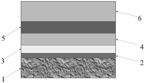
[0034] Example 1: 1) At 450, ℃ in argon and hydrogen environment, the die-casting aluminum mold is subjected to plasma etching; 2) Then under the condition of 0.02Pa, -800V, Cr is evaporated from the Cr target at high temperature and heated at high bias Under pressure, make it move to the surface of the mold at high speed, so as to deposit a 1 nanometer thick transition metal Cr binding layer on the surface of the mold;
[0035] 3) Under the conditions of 0.5Pa and -50V, feed nitrogen to react with Cr, and deposit a 50 nm thick CrN transition layer on the surface of the mold;
[0036] 4) Under the conditions of 2Pa and -100V, release AlCrSi on the AlCrSi target to react with the CrN transition layer, and deposit a 40nm CrN / AlCrSiN support layer on the surface of the mold;
[0037] 5) Under the conditions of 3Pa and -100V, control the on-off of oxygen and nitrogen to deposit and generate a 100 nanometer thick AlCrSiN / AlCrSiON hardening layer on the surface of the mold;
[0038...
Embodiment 2
[0040] Example 2: 1) After plasma etching the die-casting aluminum mold at 550°C in an argon and hydrogen environment, 2) under the conditions of 0.4Pa and -1000V, Cr was evaporated from the Cr target at high temperature and heated at high temperature. Under the action of bias voltage, make it move to the surface of the mold at high speed, so as to deposit a 40 nanometer thick transition metal Cr binding layer on the surface of the mold;
[0041] 3) Under the conditions of 2Pa and -300V, feed nitrogen to react with Cr, and deposit a 2000 nanometer thick CrN transition layer on the surface of the mold;
[0042] 4) Under the conditions of 2.5Pa and -250V, release AlCrSi on the AlCrSi target to react with the CrN transition layer to deposit a 2000 nm thick CrN / AlCrSiN support layer on the mold surface;
[0043] 5) Under the conditions of 3Pa and -300V, control the on-off of oxygen and nitrogen to deposit and generate a 2400 nanometer thick AlCrSiN / AlCrSiON hardening layer on the ...
Embodiment 3
[0046] Example 3: 1) After plasma etching the die-casting aluminum mold at 500°C in an argon and hydrogen environment, 2) under the conditions of 0.2Pa and -800V, evaporate Cr from the Cr target at a high temperature and Under the action of bias voltage, make it move to the surface of the mold at high speed, so as to deposit a 20 nanometer thick transition metal Cr binding layer on the surface of the mold;
[0047] 3) Under the conditions of 1Pa and -100V, feed nitrogen to react with Cr, and deposit a CrN transition layer with a thickness of 1000 nanometers on the surface of the mold;
[0048] 4) Under the conditions of 3Pa and -150V, release AlCrSi on the AlCrSi target to react with the CrN transition layer to deposit a 1000 nm thick CrN / AlCrSiN support layer on the surface of the mold;
[0049] 5) Under the conditions of 4Pa and -200V, control the on-off of oxygen and nitrogen to deposit a 1000 nanometer thick AlCrSiN / AlCrSiON hardening layer on the surface of the mold;
[...
PUM
| Property | Measurement | Unit |
|---|---|---|
| hardness | aaaaa | aaaaa |
| hardness | aaaaa | aaaaa |
| hardness | aaaaa | aaaaa |
Abstract
Description
Claims
Application Information
 - R&D
- Intellectual Property
- Life Sciences
- Materials
- Tech Scout
- Unparalleled Data Quality
- Higher Quality Content
- 60% Fewer Hallucinations
Browse by: Latest US Patents, China's latest patents, Technical Efficacy Thesaurus, Application Domain, Technology Topic, Popular Technical Reports.
© 2025 PatSnap. All rights reserved.Legal|Privacy policy|Modern Slavery Act Transparency Statement|Sitemap|About US| Contact US: help@patsnap.com


