Device and method for preparing or treating thin film assisted by pulsed electric field
A technology of thin film treatment and treatment method, applied in metal material coating process, vacuum evaporation plating, coating and other directions, can solve the problems of performance degradation, slow heating, slow cooling, etc.
- Summary
- Abstract
- Description
- Claims
- Application Information
AI Technical Summary
Problems solved by technology
Method used
Image
Examples
Embodiment 1
[0057] Preparation of TiAlN coating under pulsed electric field
[0058] Step 1, cleaning of the substrate
[0059] After grinding and polishing the tungsten carbide sheet, use acetone and alcohol to ultrasonically clean the sapphire substrate for 15 minutes. After cleaning, use high-purity inert gas to dry it. Use a pulse electric field clamp to fix the substrate and put it into a vacuum chamber.
[0060] Step 2, preparation of TiAlN coating under pulsed electric field
[0061] Using the same preparation conditions as in Comparative Example 1, a pulse current was connected during the preparation process to prepare a TiAlN coating under a pulse electric field. Among them, the pulse current intensity is 15A, the pulse width is 10s, and the processing time is 5-10min.
[0062] Step 3, turn off the magnetron sputtering equipment, take out the sample after degassing, put it into a centrifuge tube, and inject inert high-purity Ar for subsequent detection.
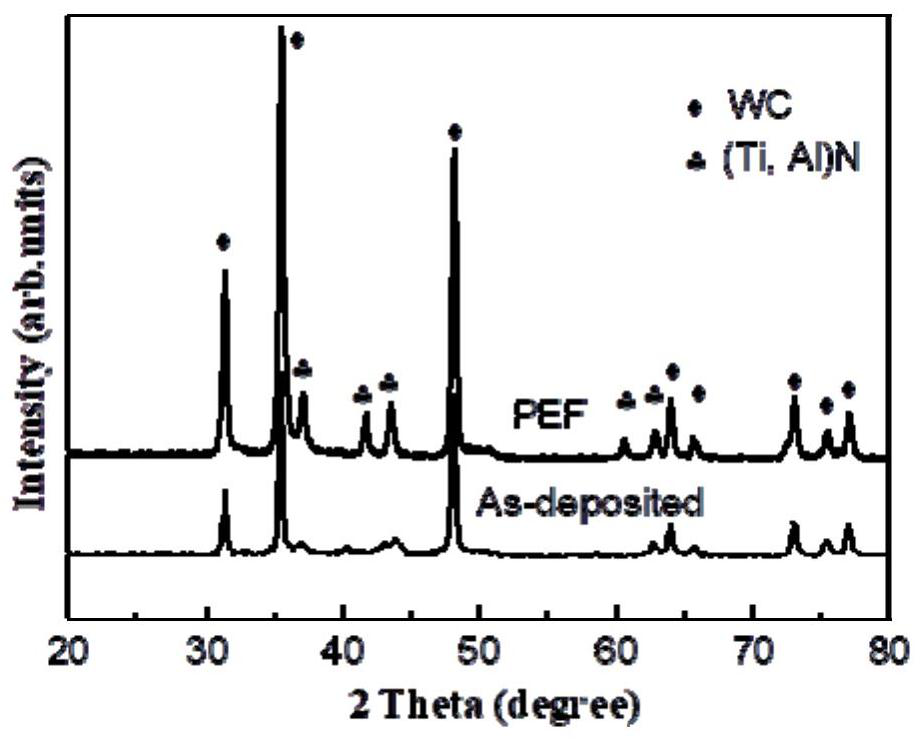
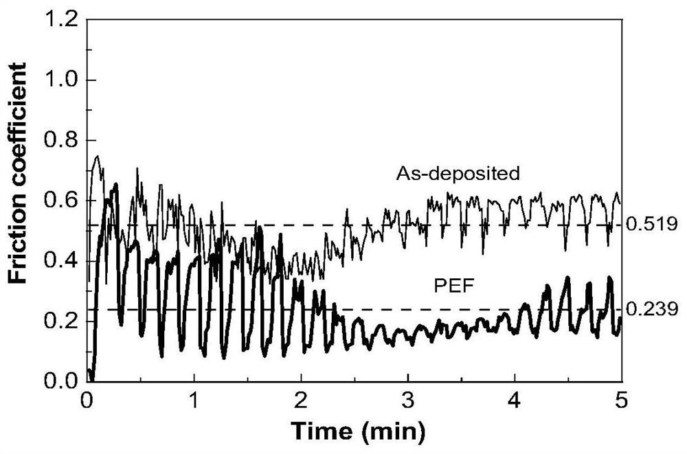
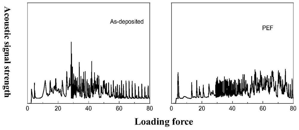
[0063] figure 1 XRD ...
Embodiment 2
[0078] Oxidation Treatment of Ca-Co Thin Films Using Pulse Electric Field
[0079] Step 1, connect the circuit
[0080] Use a clamp to fix the film, and connect the clamp and the pulse current generator to form a closed loop.
[0081] Step 2, pulsed electric field oxidation treatment of Ca-Co film
[0082] After setting the pulse electric field pulse current 0.01A, pulse width 1s, pulse rise time 0.05A / s and other parameters, start processing, processing time 1h.
[0083] Step 3, end of processing, take out the sample
[0084] After the timing is over, the sample is taken out, put into a centrifuge tube, and passed through inert high-purity Ar for subsequent detection.
[0085] Figure 6 It is a comparison chart of the XRD diffraction pattern of Co-Ca in Example 2 when it is oxidized by a pulsed electric field and Comparative Example 3 when it is oxidized by a tube furnace.
[0086] From the XRD diffraction pattern, it can be found that the Co-Ca compound can be oxidized ...
Embodiment 3
[0096] Pulsed electric field heat treatment of Bi 2 Te 3 film
[0097] Step 1, connect the circuit
[0098] Use a clamp to fix the film, and connect the clamp and the pulse current generator to form a closed loop. Fix the thermocouple above the film and connect the temperature collector to the display.
[0099] Step 2, pulsed electric field heat treatment of Bi 2 Te 3 film
[0100] After setting the pulse electric field pulse current 0.05A, pulse width 1s, pulse rise time 0.05A / s and other parameters, start processing, processing time 1h, and collect temperature changes at the same time.
[0101] Step 3, end of processing, take out the sample
[0102] After the timing is over, the sample is taken out, put into a centrifuge tube, and passed through inert high-purity Ar for subsequent detection.
[0103] Figure 8 Deposited Bi prepared for Comparative Example 4 2 Te 3 Film and the Bi after pulse electric field heat treatment of embodiment 3 2 Te 3 SEM comparison ima...
PUM
| Property | Measurement | Unit |
|---|---|---|
| dispersion coefficient | aaaaa | aaaaa |
| dispersion coefficient | aaaaa | aaaaa |
Abstract
Description
Claims
Application Information
 - R&D
- Intellectual Property
- Life Sciences
- Materials
- Tech Scout
- Unparalleled Data Quality
- Higher Quality Content
- 60% Fewer Hallucinations
Browse by: Latest US Patents, China's latest patents, Technical Efficacy Thesaurus, Application Domain, Technology Topic, Popular Technical Reports.
© 2025 PatSnap. All rights reserved.Legal|Privacy policy|Modern Slavery Act Transparency Statement|Sitemap|About US| Contact US: help@patsnap.com


