
Piezoelectric tunneling transistor and operation mode control method thereof

A technology of tunneling transistor and working mode, which is applied in semiconductor/solid-state device manufacturing, piezoelectric/electrostrictive/magnetostrictive devices, circuits, etc., which can solve the problems of increased power consumption density and achieve low off-state current, The effect of high on-state current and high performance

Inactive Publication Date: 2019-09-24
INST OF SEMICONDUCTORS - CHINESE ACAD OF SCI
View PDF3 Cites 0 Cited by
  • Summary
  • Abstract
  • Description
  • Claims
  • Application Information

AI Technical Summary

Problems solved by technology

At the same time, the operating voltage and threshold voltage of the device are also required to be continuously reduced to avoid the increase in power consumption density caused by the increase in integration
But in the traditional field effect transistor MOSFET, the turn-off and turn-on of the current is related to the ability of hot electrons to cross the energy band barrier, and the transmission slope (subthreshold swing) of the current from the off state to the on state is subject to the Boltzmann The limit, which is commonly referred to as the Boltzmann tyranny, the limit value of the subthreshold swing of traditional MOSFETs at room temperature is 60mV / decade

Method used


Image

  • Piezoelectric tunneling transistor and operation mode control method thereof
  • Piezoelectric tunneling transistor and operation mode control method thereof
  • Piezoelectric tunneling transistor and operation mode control method thereof

Examples


Embodiment Construction

[0037] In order to make the object, technical solution and advantages of the present invention clearer, the present invention will be further described in detail below in conjunction with specific embodiments and with reference to the accompanying drawings.

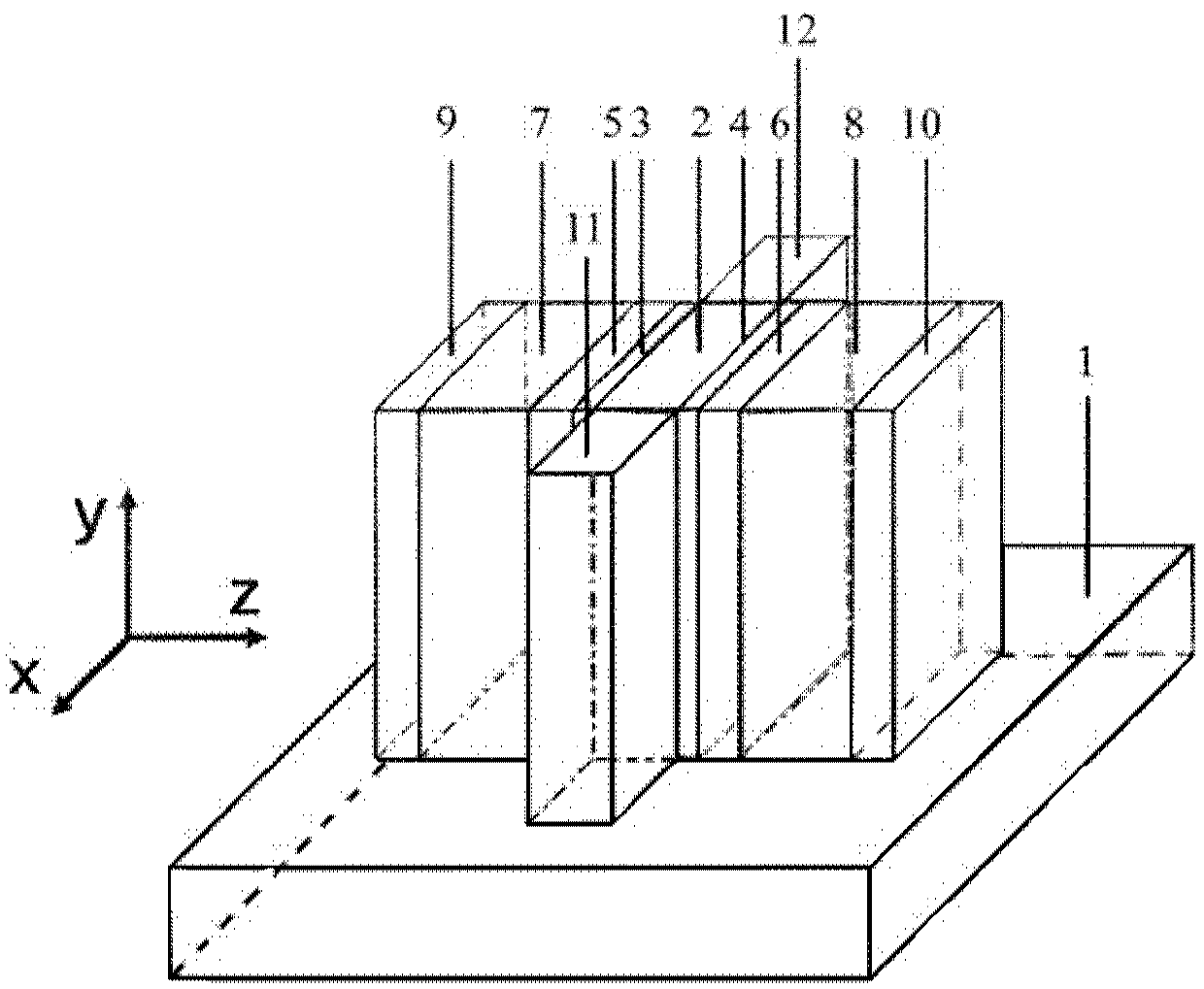
[0038] According to one aspect of the present invention, a piezoelectric tunneling transistor is provided, such as figure 1 shown, including:

[0039] semiconductor substrate 1;

[0040] The semiconductor channel 2 is placed on the upper surface of the semiconductor substrate 1;

[0041] The gate dielectric layers 3 and 4 are placed symmetrically on both sides of the semiconductor channel 2, respectively;

[0042] The control gate electrodes 5, 6 are placed symmetrically outside the gate dielectric layers 3, 4, respectively;

[0043] Piezoelectric layers 7, 8 are placed symmetrically outside the control grid electrodes 5, 6, respectively;

[0044] Piezoelectric grid electrodes 9, 10 are placed symmetrically outside th...


PUM


Abstract

The invention provides a piezoelectric tunneling transistor and an operation mode control method thereof, and belongs to the technical field of transistors. The piezoelectric tunneling transistor comprises a semiconductor substrate; a semiconductor channel which is arranged on the upper surface of the semiconductor substrate; two gate dielectric layers which are symmetrically arranged on the two sides of the semiconductor material channel; two control gate electrodes which are symmetrically arranged on the outer side of the two gate dielectric layers; two piezoelectric layers which are symmetrically arranged on the outer side of the two control gate electrodes; two piezoelectric gate electrodes which are symmetrically arranged on the outer side of the two piezoelectric layers; and doped semiconductors which are used as the source end and the drain end and are symmetrically arranged on the other two sides of the semiconductor material channel. The piezoelectric tunneling transistor is symmetrically distributed with the semiconductor channel as the axis, and the two ends of the piezoelectric layers can generate a bias voltage change to the semiconductor channel so as to improve the on-state and off-state current of the piezoelectric tunneling transistor.

Description

technical field [0001] The invention relates to the field of transistors, in particular to a piezoelectric tunneling transistor and a method for controlling its working mode. Background technique [0002] With the continuous improvement of integration, the feature size of traditional metal oxide semiconductor devices has been continuously reduced, and has approached its miniaturization limit. At the same time, the operating voltage and threshold voltage of the device are also required to be continuously reduced to avoid the increase in power consumption density caused by the increase in integration. But in the traditional field effect transistor MOSFET, the turn-off and turn-on of the current is related to the ability of hot electrons to cross the energy band barrier, and the transmission slope (subthreshold swing) of the current from the off state to the on state is subject to the Boltzmann The limit, which is commonly referred to as the Boltzmann tyranny, has a limit of 6...

Claims


Application Information

Patent Timeline
Patent Type & Authority Applications(China)
IPC IPC(8): H01L29/06H01L29/423H01L21/336H01L41/113H10N30/30
CPCH01L29/0688H01L29/423H01L29/66409H10N30/30
Inventor 龙宇雄文宏玉姜向伟
Owner INST OF SEMICONDUCTORS - CHINESE ACAD OF SCI
Learn More