
Logic Expression Extraction and Switch Level Design Method for CMOS Transmission Gate Logic Circuit

A logic expression and logic circuit technology, applied in CAD circuit design, design optimization/simulation, etc., can solve the problems of reduced process feature size, increased static power consumption of MOS tubes, etc., and achieves fewer MOS tubes and lower power consumption Power consumption, the effect of saving chip area

Active Publication Date: 2022-03-22
HUAIBEI NORMAL UNIVERSITY
View PDF2 Cites 0 Cited by
  • Summary
  • Abstract
  • Description
  • Claims
  • Application Information

AI Technical Summary

Problems solved by technology

[0016] (2) The power supply voltage of the circuit is reduced, which reduces the dynamic power consumption; but the process feature size is reduced, so that the threshold voltage of the MOS transistor and the thickness of the gate oxide layer are correspondingly reduced, and the subthreshold value generated by the subthreshold (weak inversion) conduction of the MOS transistor The static power consumption of the MOS tube caused by leakage current and gate leakage current increases, and the reduction of power consumption should consider reducing dynamic power consumption and reducing static power consumption
It can be seen that there is a contradiction between saving area, reducing power consumption and increasing speed

Method used


Image

  • Logic Expression Extraction and Switch Level Design Method for CMOS Transmission Gate Logic Circuit
  • Logic Expression Extraction and Switch Level Design Method for CMOS Transmission Gate Logic Circuit
  • Logic Expression Extraction and Switch Level Design Method for CMOS Transmission Gate Logic Circuit

Examples


Embodiment 1

[0074] A logical expression extraction and switch-level design method for a CMOS transmission gate logic circuit expands the Boolean algebra system to obtain an extended Boolean algebra system; a corresponding switch-level signal flow graph model is established by the CMOS transmission gate logic circuit, thereby The equivalent signal flow graph model of the output function of the circuit is extracted from the model, and the switch-level function expression of the circuit is obtained by combining the switch-level signal flow graph model with the extended Boolean algebra system, and thus the CMOS transmission gate logic circuit is obtained.

[0075] The number of MOS transistors contained in the circuit is still an important indicator to measure the power consumption and area of ​​the circuit. The study found that using the full-swing CMOS transmission gate circuit structure can avoid threshold voltage loss, reduce sub-threshold power consumption, and reduce the number of MOS tr...

Embodiment 2

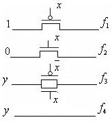
[0113] like figure 1 As shown, there are four types of component branches of the CMOS transmission gate circuit, namely, the PMOS tube branch, the NMOS tube branch, the CMOS transmission gate branch and the connection branch, wherein the PMOS tube and the NMOS tube are single-channel transmission gates, The 1 signal and the 0 signal can be transmitted without loss, respectively, and the CMOS transmission gate branch is a dual-channel transmission gate, which can transmit signal variables without loss. The above three types of branches are all controlled branches, and the connecting branches are uncontrolled branches, that is, direct transmission (through) branches. The switch-level function expressions of the four types of component branches are respectively

[0114]

[0115] Its corresponding switch-level signal flow graph model, such as figure 2shown. The arrow on the branch indicates the transmission (flow) direction of the signal, and the switch variable (or switch ...

Embodiment 3

[0126] like Figure 7 As shown, the CMOS transmission gate type full adder circuit (the circuit name is EX2) obtained by using the switch-signal theory design method. Use the equivalent signal flow graph model method to find the logic function expression of the circuit.

[0127] Step1 modeling. Depend on Figure 7 For the full adder circuit shown, draw the signal flow graph model of the complement function of the output function of the circuit as Figure 8 shown. In the figure, C(0) means C=0, express and many more. Depend on Figure 8 ,use and The signal flow diagram of the transmission 0 signal is transformed to obtain the output function s of the circuit i , c i and the equivalent signal flow graph model of h as Figure 9 shown.

[0128] Step2 analysis. Depend on Figure 9 The output s of the full adder can be obtained directly i and c i for

[0129]

[0130] After simplification by Boolean algebra (signal algebra) method, the logical expression of ...


PUM


Abstract

The invention discloses a logical expression extraction and switch-level design method of a CMOS transmission gate logic circuit, which expands the Boolean algebra system to obtain the extended Boolean algebra system; the corresponding switch-level signal flow diagram is established by the CMOS transmission gate logic circuit From this model, the equivalent signal flow graph model of the output function of the circuit is extracted, and the switch-level function expression of the circuit is obtained by combining the switch-level signal flow graph model with the extended Boolean algebra system, thereby obtaining the CMOS transmission gate logic circuit . The CMOS transmission gate logic circuit designed by the method of the present invention requires less MOS tubes and fewer connections, which can reduce power consumption and save chip area; and the designed switching level CMOS transmission gate logic circuit It is full-swing and suitable for the design of low-power CMOS circuits.

Description

technical field [0001] The invention relates to a logic expression extraction and switch level design method of a logic circuit, in particular to a logic expression extraction and switch level design method of a CMOS transmission gate logic circuit. Background technique [0002] Complementary metal-oxide semiconductor (CMOS) integrated circuits are widely used in very large-scale integrated circuits (VLSI) because of their low power consumption, high integration, strong anti-interference ability, and wide power supply voltage range. Among them, logic circuits composed of various combinations of CMOS transmission gates have become a wider circuit form. Studies have shown that a simpler circuit structure can often be obtained by using the switch-level design method. This circuit structure is a CMOS transmission gate logic circuit composed of various combinations of CMOS transmission gates. [0003] However, how to extract the corresponding logic functions from the actual or d...

Claims


Application Information

Patent Timeline
Patent Type & Authority Patents(China)
IPC IPC(8): G06F30/39G06F30/20
CPCG06F30/39G06F30/20
Inventor 姜恩华
Owner HUAIBEI NORMAL UNIVERSITY
Learn More