Up-conversion photo-emission photoelectric transistor and preparation method thereof and application of up-conversion photo-emission photoelectric transistor
A phototransistor and light conversion technology, applied in circuits, electrical components, semiconductor devices, etc., can solve the problems of low luminous contrast of devices, reduced device efficiency, high material cost and equipment cost, and achieve high luminous contrast of devices and improved luminous contrast. , the effect of low production cost
- Summary
- Abstract
- Description
- Claims
- Application Information
AI Technical Summary
Problems solved by technology
Method used
Image

Examples
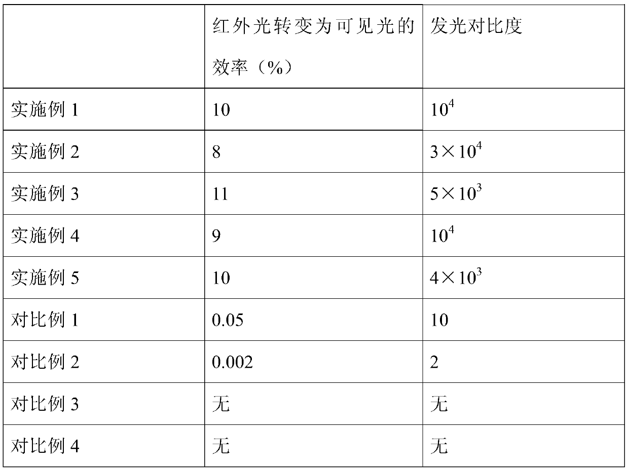
Embodiment 1
[0075] In this embodiment, an up-conversion light-emitting phototransistor is prepared according to the following method:
[0076] The ITO substrate with the electrode pattern is used as the first transparent conductive electrode to undergo the following ultrasonic cleaning steps: sequentially use acetone, isopropanol, and deionized water for 8 minutes, take it out and dry it for later use. After the dried ITO substrate was treated with ultraviolet ozone for 10 minutes, it was taken out and then spin-coated with ZnO nanoparticles and PbS quantum dots in a nitrogen-filled glove box, wherein the concentrations of ZnO nanoparticles and PbS quantum dots were 30 mg / mL and 50mg / mL, spin at 1500r / min and 2500r / min for 30 seconds, bake at 120°C and 90°C for 10 minutes, respectively, to form a hole blocking layer and an infrared absorbing layer, in which PbS needs to be repeatedly spin-coated 5 layers . The dielectric layer is made of PVP with a concentration of 100mg / mL, spin-coated ...
Embodiment 2
[0082] In this embodiment, an up-conversion light-emitting phototransistor is prepared according to the following method:
[0083] With the ITO sheet whose square resistance is 15 Ω / sq as the substrate (the third transparent conductive electrode), use deionized water, acetone and isopropanol to ultrasonically each for 15 minutes, and then place them in a vacuum oven (O 2 2 O<1p.p.m.), and the dried ITO substrate was treated with plasma for 1 minute. Spin-coat lithium fluoride, ZnO nanoparticles, CdSe / ZnS quantum dots (10 mg / mL in n-hexane) and poly(9,9-dioctylfluorene-CO-N-(4-butyl) sequentially in a glove box Phenyl)diphenylamine) (in chlorobenzene, 8mg / mL), the rotation speed is 2000r / min, 2000r / min, 2500r / min or 3000r / min, and baked at 90°C for 10 minutes, 10 minutes, 10 minutes respectively minutes and 30 minutes to form an electron injection layer, an electron transport layer, a light emitting layer and a hole transport layer. Then spin-coat PEDOT:PSS (3500r / min, 40 sec...
Embodiment 3
[0089] In this embodiment, an up-conversion light-emitting phototransistor is prepared according to the following method:
[0090] The ITO sheet with a square resistance of 15Ω / sq is used as the substrate (the first transparent conductive electrode). Before use, the ITO substrate needs to be thoroughly ultrasonically cleaned in detergent, deionized water, acetone and isopropanol in sequence. The substrate was dried with nitrogen and treated with UV-ozone for 15 minutes. Take out and spin-coat ZnO nanoparticles and carbon nanotubes sequentially in a glove box full of nitrogen, wherein the concentrations of ZnO nanoparticles and carbon nanotubes are 30mg / mL and 60mg / mL, respectively, at 1500r / min and 3000r / min After rotating for 30 seconds, bake at 120°C and 90°C for 10 minutes respectively to form a hole blocking layer and an infrared absorbing layer, in which carbon nanotubes need to be spin-coated repeatedly for 4 layers. The dielectric layer is made of PVP with a concentrat...
PUM
 Abstract
Description
Claims
Application Information
 - R&D
- Intellectual Property
- Life Sciences
- Materials
- Tech Scout
- Unparalleled Data Quality
- Higher Quality Content
- 60% Fewer Hallucinations
Browse by: Latest US Patents, China's latest patents, Technical Efficacy Thesaurus, Application Domain, Technology Topic, Popular Technical Reports.
© 2025 PatSnap. All rights reserved.Legal|Privacy policy|Modern Slavery Act Transparency Statement|Sitemap|About US| Contact US: help@patsnap.com