


Quick Research
Generate reliable direction feasibility study reports for your R&D in just a few steps.

Technical Q&A
Discover and master advanced knowledge NOW. Basics, ideas, possibilities, all at once.

Find Solutions
As an expert in R&D theories, this can generate solutions to your technical problems instantly.

Evaluate Feasibility
Analyze your overall solution with one click, know your potential R&D risks in advance.

Monitor Landscape
Get weekly tech updates, stay abreast of the latest tech innovations and key insights.
Quantum anomalous Hall effect thin-film microstructural device and preparation method thereof
An abnormal Hall effect and microstructure technology, applied in the field of electronic information, can solve the problems of compound film material damage, difficulty in developing time control, etc., and achieve the effect of avoiding corrosion
- Summary
- Abstract
- Description
- Claims
- Application Information
AI Technical Summary
Problems solved by technology
Method used
Image

Examples
preparation example Construction
[0046] A method for preparing a quantum anomalous Hall effect thin film microstructure device, the specific steps are as follows:
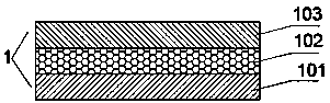
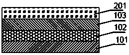
[0047] 1) Evenly coated protective layer: Al in topological insulator material 1 2 o 3 Layer 103 is evenly coated with electron beam glue as the protective layer 201; the electron beam glue is PMMA electron beam glue with a thickness of 100-120nm; last for 50-60s; if figure 2 shown;
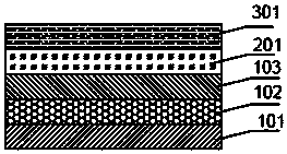
[0048] 2) Uniform coating of UV photoresist: Uniform coating of UV positive photoresist 301 on the protective layer 201; the thickness of the UV positive photoresist is 800-900nm, and the uniform coating process conditions are: the speed is 600r / min for 6 -8s, at 4000r / min for 50-60s, harden the photoresist film layer on the rubber baking table, set the temperature at 85-90°C, and the time is 260-300s; image 3 shown;
[0049] 3) Single-layer photolithography: transfer the pattern of the mask to the UV positive photoresist 301 by photolithography process; the e...
Embodiment 1
[0062] A method for preparing a quantum anomalous Hall effect thin film microstructure device, the specific steps are as follows:
[0063] 1) Evenly coated protective layer: Al in topological insulator material 1 2 o 3 Layer 103 is uniformly coated with electron beam glue as the protective layer 201; the electron beam glue is PMMA electron beam glue with a thickness of 100nm; the process conditions for uniform glue are: 600r / min at a speed of 600r / min for 6s, and 4000r / min for 50s;
[0064] 2) Uniform coating of UV photoresist: uniform coating of UV positive photoresist 301 on the protective layer 201; the thickness of the UV positive photoresist is 800nm, and the uniform coating process conditions are: 600r / min at a speed of 6s, 4000r Continue for 50s at the rotation speed of / min, and harden the photoresist film layer on the rubber baking table, set the temperature at 85°C, and the time is 260s;
[0065] 3) Single-layer photolithography: transfer the pattern of the mask to...
Embodiment 2
[0070] A method for preparing a quantum anomalous Hall effect thin film microstructure device, the specific steps are as follows:
[0071] 1) Evenly coated protective layer: Al in topological insulator material 1 2 o 3 Layer 103 is evenly coated with electron beam glue as the protective layer 201; the electron beam glue is PMMA electron beam glue with a thickness of 105nm; the process conditions for uniform glue are: the speed of 600r / min lasts for 7s, and the speed of 4000r / min lasts for 52s;
[0072] 2) Uniform coating of UV photoresist: uniform coating of UV positive photoresist 301 on the protective layer 201; the thickness of the UV positive photoresist is 820nm, and the uniform coating process conditions are: 600r / min for 7s, 4000r Continue for 52s at the speed of / min, and harden the photoresist film layer on the rubber baking table, set the temperature at 86°C, and the time is 270s;
[0073] 3) Single-layer photolithography: transfer the pattern of the mask to the UV...
PUM
| Property | Measurement | Unit |
|---|---|---|
| Thickness | aaaaa | aaaaa |
| Thickness | aaaaa | aaaaa |
| Thickness | aaaaa | aaaaa |
Abstract
Description
Claims
Application Information
 - R&D Engineer
- R&D Manager
- IP Professional
- Industry Leading Data Capabilities
- Powerful AI technology
- Patent DNA Extraction
Browse by: Latest US Patents, China's latest patents, Technical Efficacy Thesaurus, Application Domain, Technology Topic, Popular Technical Reports.
© 2024 PatSnap. All rights reserved.Legal|Privacy policy|Modern Slavery Act Transparency Statement|Sitemap|About US| Contact US: help@patsnap.com