Preparation method of high-performance conductive nano ceramic metal clad coating on pure copper surface
A technology of ceramic metal and conductive nano, which is applied in the coating process and coating of metal materials, which can solve the problems of increased coating pores and enhanced phase agglomeration, and achieve the effects of reducing pores, avoiding agglomeration, and good electrical conductivity
- Summary
- Abstract
- Description
- Claims
- Application Information
AI Technical Summary
Problems solved by technology
Method used
Image
Examples
Embodiment 1
[0024] Take a piece of 20mm×20mm×15mm industrial pure copper, and use its 20mm×20mm surface as the experimental surface. First, polish the surface of the pure copper substrate with 150# sandpaper to remove the oxide layer and other impurities on the surface of the substrate. Then place it in absolute ethanol and acetone and ultrasonically clean it for 5 minutes to clean off the oil stains remaining on the surface of the substrate. Finally, air-dry and paint with ink for blackening treatment.
[0025] Add 2000ml of 0.1mol / L ZrOCl into the beaker 2 Solution, under magnetic stirring, 1000ml of 0.2mol / LNaBH 4 The solution is dripped into a beaker, reacted to obtain a white sol, filtered out the sol, and washed 3 times with absolute ethanol to obtain Zr(OH) 4 gel.
[0026] Weigh 31.3g Zr(OH) 4 Gel, 80g Cu powder, 12.4g B 2 o 3 The powder and 10.6 g of graphite were uniformly mixed to obtain a coating material. The coating material is evenly coated on the surface of the pure ...
Embodiment 2
[0039] According to the method of Example 1, the surface of the 20mm × 20mm × 15mm pure copper substrate is pretreated, and Zr(OH) 4 gel.
[0040] Weigh 28.1g Zr(OH) 4 Gel, 82g Cu powder, 11.1g B 2 o 3 Powder and 9.5g of graphite were mixed evenly to obtain a coating material. The coating material is evenly coated on the surface of the pure copper substrate with a coating thickness of 3 mm to form a layer to be clad.
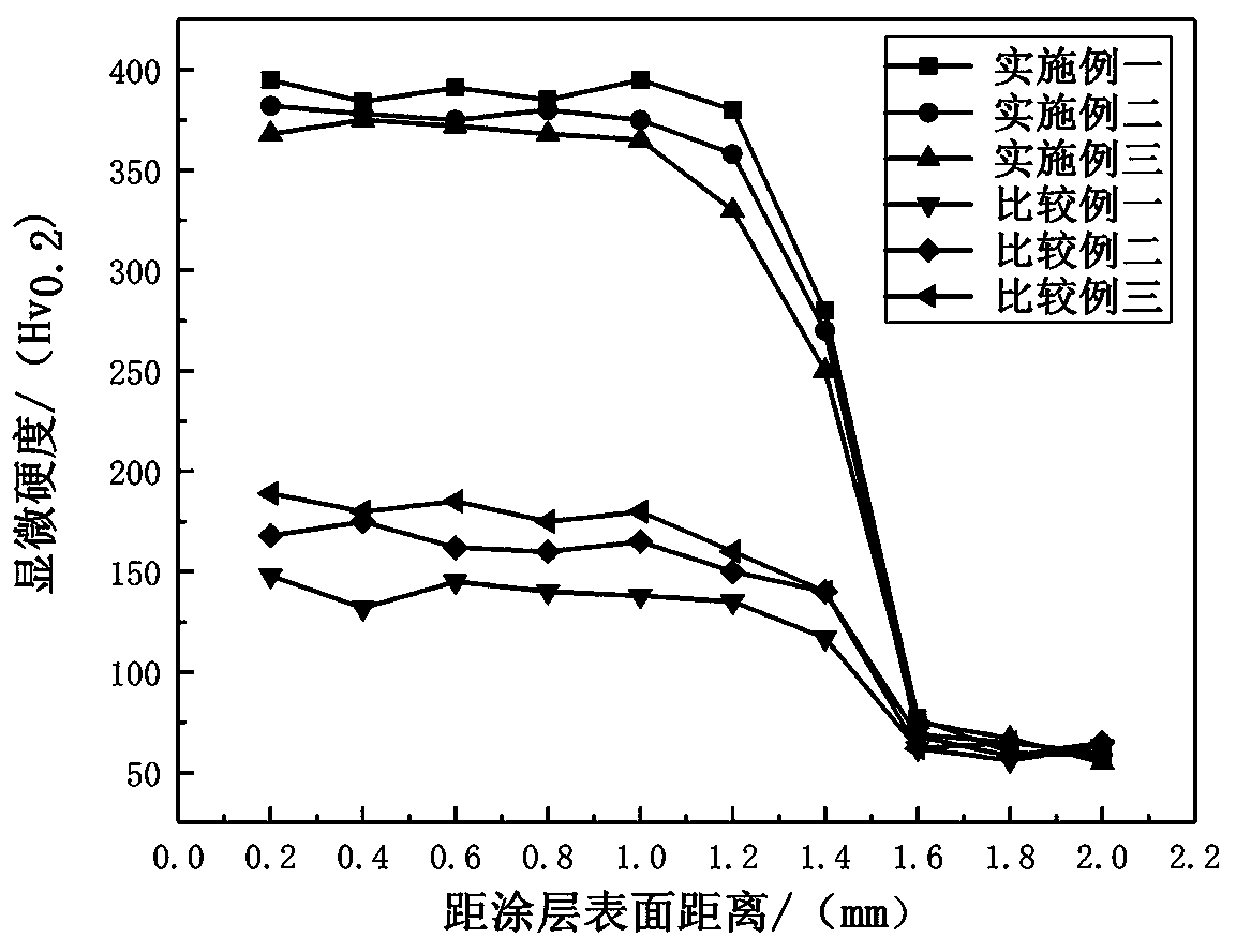
[0041] Set the laser power of the semiconductor laser to 2800W, the spot diameter to 4mm, the flow rate of argon gas to 15L / min, and the overlap rate to 50%. Aim the laser head of the semiconductor laser at the layer to be clad, and follow the set track at a rate of 2mm / s. The scanning speed continuously scans the layer to be clad, and forms ZrB on the surface of the pure copper substrate 2 1.5mm thick nano-ZrB with 18wt% content 2 / Cu ceramic metal cladding coating.
[0042] The hardness, electrical conductivity and tensile strength of the cladding coati...
Embodiment 3
[0047] According to the method of Example 1, the surface of the 20mm × 20mm × 15mm pure copper substrate is pretreated, and Zr(OH) 4 gel.
[0048] Weigh 25g Zr(OH) 4 Gel, 84g Cu powder, 9.9g B 2 o 3 The powder and 8.5g of graphite are mixed and evenly coated on the surface of the pure copper substrate with a coating thickness of 3mm to form a layer to be clad.
[0049] Set the laser power of the semiconductor laser to 2800W, the spot diameter to 4mm, the flow rate of argon gas to 15L / min, and the overlap rate to 50%. Aim the laser head of the semiconductor laser at the layer to be clad, and follow the set track at a rate of 3mm / s. The scanning speed continuously scans the layer to be clad, and forms ZrB on the surface of the pure copper substrate 2 1.5mm thick nano-ZrB with 16wt% content 2 / Cu ceramic metal cladding coating.
[0050] The hardness, electrical conductivity and tensile strength of the cladding coating were detected according to the test method of Example 1....
PUM
| Property | Measurement | Unit |
|---|---|---|
| particle diameter | aaaaa | aaaaa |
| tensile strength | aaaaa | aaaaa |
| thickness | aaaaa | aaaaa |
Abstract
Description
Claims
Application Information
 - R&D
- Intellectual Property
- Life Sciences
- Materials
- Tech Scout
- Unparalleled Data Quality
- Higher Quality Content
- 60% Fewer Hallucinations
Browse by: Latest US Patents, China's latest patents, Technical Efficacy Thesaurus, Application Domain, Technology Topic, Popular Technical Reports.
© 2025 PatSnap. All rights reserved.Legal|Privacy policy|Modern Slavery Act Transparency Statement|Sitemap|About US| Contact US: help@patsnap.com


