Ultrasound-assisted column implanting method for CuCGA (Ceramic Copper Column Grid Array) device packaging
An ultrasonic-assisted and device packaging technology, which is applied to the assembly of printed circuits with electrical components, electrical solid devices, semiconductor devices, etc., can solve the problems of difficulty in planting copper columns in arrays, great influence on the quality of planting columns, and poor heat transfer in welding.
- Summary
- Abstract
- Description
- Claims
- Application Information
AI Technical Summary
Problems solved by technology
Method used
Image
Examples
specific Embodiment approach 1
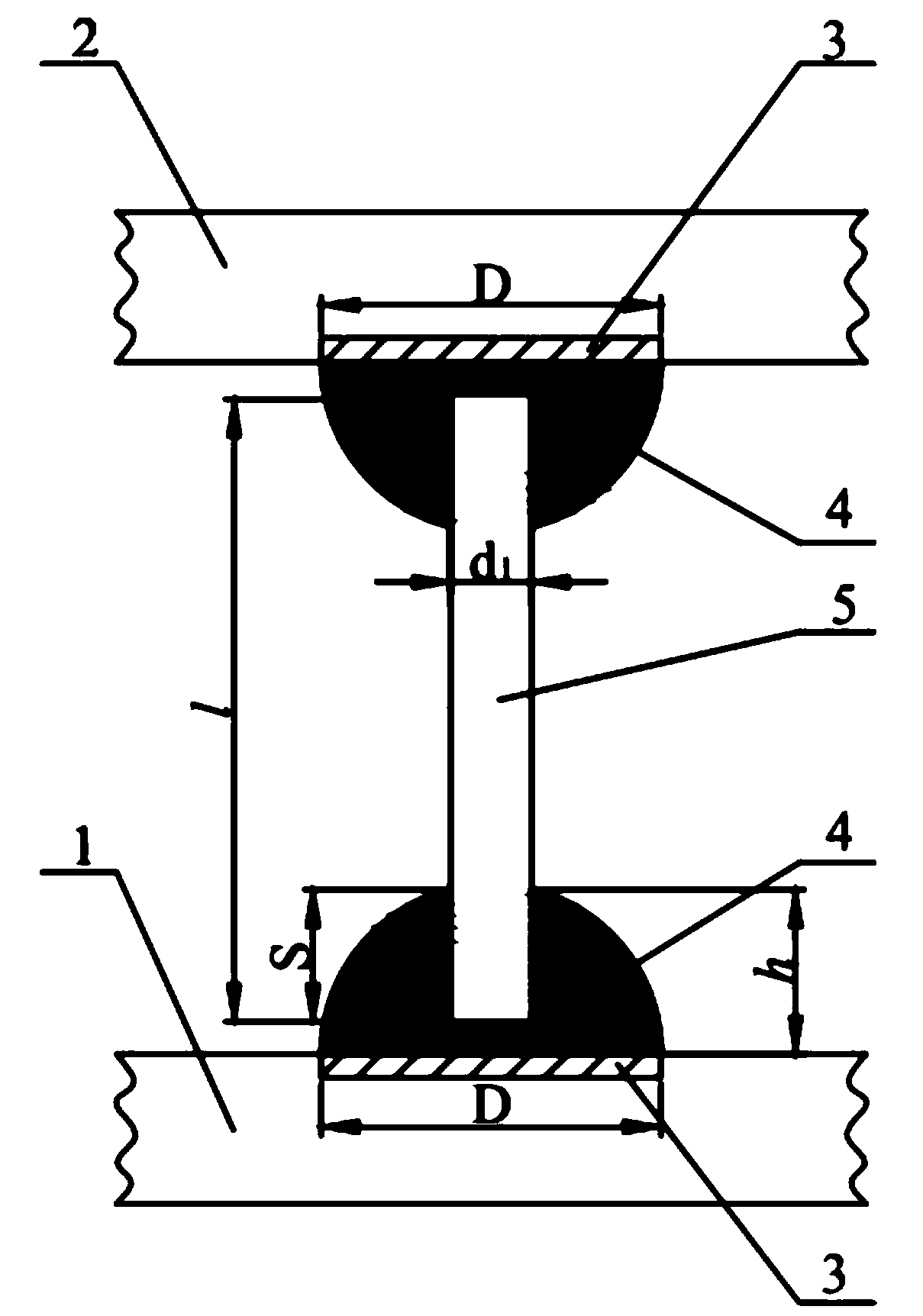
[0044] A method for ultrasonically assisted pillar planting for CuCGA device packaging, comprising the following steps:
[0045] Step 1. Print solder paste with non-eutectic solder composition on the arrayed pads:
[0046] Same as the traditional BGA ball planting process, a sufficient amount of non-eutectic solder paste is printed on the arrayed pads of the printed circuit board and the chip carrier substrate by means of a mature stencil printing process;
[0047] Step 2. Realize the ball planting on the pads arranged in an array on the printed circuit board and the chip carrier substrate by reflow soldering:
[0048] The solder paste on the pads arranged in an array on the printed circuit board and the chip carrier substrate is heated and melted, the flux in the solder paste removes the oxide film on the pads, the solder in the solder paste wets the pads, and Solder balls arranged in an array are formed under the action of surface tension;
[0049] Step 3. Form a positioni...
specific Embodiment approach 2
[0059] The material of the pads arranged in an array in this embodiment is any one of copper, gold, silver, nickel, tin bronze, and brass, or a combination of copper, gold, silver, nickel, tin bronze, and brass The combined multi-layer metal film pad can also be one of the metals or alloys on which other tin-based solders can wet well.
[0060] Other steps and parameters are the same as those in the first embodiment.
specific Embodiment approach 3
[0062] The diameter of the pads arranged in an array in this embodiment is D, where 0.9mm≤D≤3mm, and the thickness of the pads arranged in an array is 35 μm˜100 μm.
[0063] Other steps and parameters are the same as those in Embodiment 1 or 2.
PUM
 Abstract
Description
Claims
Application Information
 - R&D Engineer
- R&D Manager
- IP Professional
- Industry Leading Data Capabilities
- Powerful AI technology
- Patent DNA Extraction
Browse by: Latest US Patents, China's latest patents, Technical Efficacy Thesaurus, Application Domain, Technology Topic, Popular Technical Reports.
© 2024 PatSnap. All rights reserved.Legal|Privacy policy|Modern Slavery Act Transparency Statement|Sitemap|About US| Contact US: help@patsnap.com


