Power device packaging structure and method thereof

A technology of power devices and packaging structures, which is applied in semiconductor devices, electric solid state devices, semiconductor/solid state device components, etc., and can solve the problems of single device withstand voltage value maintaining chip withstand voltage value, poor thermal management, and solder joints falling off, etc. , achieve good thermal conductivity and reliability, improve thermal management performance, and avoid chip damage

Inactive Publication Date: 2019-07-30
SHENZHEN INST OF WIDE BANDGAP SEMICON
View PDF13 Cites 2 Cited by
  • Summary
  • Abstract
  • Description
  • Claims
  • Application Information

AI Technical Summary

Problems solved by technology

[0010] (1) From the level of the overall subunit series connection, it is the same as the traditional crimping IGBT module. After stacking and series connection, it can only dissipate heat from the outside, and cannot dissipate heat from both sides of each power module unit. The total heat dissipation area is small, and the heat dissipation Poor management;
[0011] (2) The wire bonding process is still used in the internal chip connection, so the first and second solder joints still fall off, the solder layer is fatigued, and the excessive ultrasonic energy/vertical pressure during the bonding process causes damage to the inside of the chip, etc. ri...

Method used


Image

  • Power device packaging structure and method thereof
  • Power device packaging structure and method thereof
  • Power device packaging structure and method thereof

Examples


Embodiment Construction

[0056] The specific implementation manner of the present invention will be described in detail below in conjunction with the accompanying drawings.

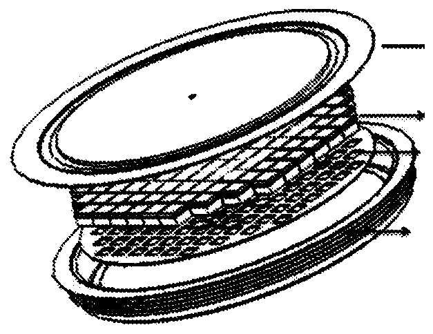
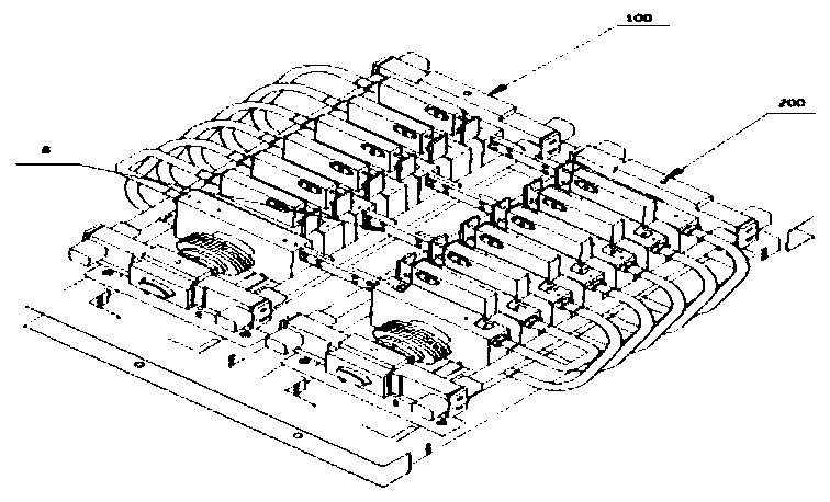
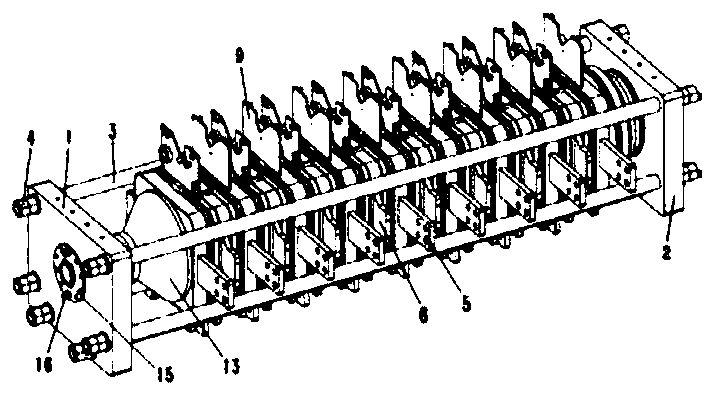
[0057] In a preferred embodiment, as Figure 5 And shown in Fig. 6 (a) and (b), the power device packaging structural unit 10 based on silver sintering technology proposed by the present invention comprises a first heat dissipation substrate 11, an IGBT transistor 12, a diode 13, a high thermal conductivity plastic casing 14 and E Font clip metal connection block 15. Wherein, the IGBT transistor 12 and the diode 13 are sintered on the surface of the long plate-type first heat dissipation substrate 11 through silver sintering technology; the metal connection blocks 15 are respectively sintered on the first heat dissipation substrate 11 through silver sintering technology, and the The IGBT transistor 12 and the diode 13 are used to realize the parallel connection of the IGBT transistor 12 and the diode 13 and the connection betwee...


PUM


Abstract

The invention provides a power device packaging structure and a preparation method thereof. The power device packaging structure comprises a plurality of power device packaging structure units, the power device packaging structure unit comprises a first heat dissipation substrate, a power device, a diode and a high-heat-conductivity plastic packaging material shell, wherein the power device and the diode are arranged on the surface of the first heat dissipation substrate, and the upper part of the power device packaging structure unit is subjected to plastic packaging by using a high-heat-conductivity plastic packaging material, a high-heat-conductivity plastic packaging material shell. The first heat dissipation substrate is in a long plate shape, and the power device and the diode are sintered on the surface of the first heat dissipation substrate through a sintering technology. The power device packaging structure based on the sintering technology can realize series-parallel connection in a two-dimensional plane, has good heat conductivity and reliability, and is simple in grid control; and in the manufacturing of a single subunit, the chip surface is not required to be directlycontacted, so that the risk of chip damage caused by uneven pressure is avoided.

Description

technical field [0001] The invention belongs to the field of semiconductor packaging devices, in particular to the field of design and manufacture of IGBT parallel power modules. Background technique [0002] IGBT (Insulated Gate Bipolar Transistor), Insulated Gate Bipolar Transistor, is a composite fully-controlled voltage-driven power semiconductor device composed of BJT (Bipolar Transistor) and MOS (Insulated Gate Field Effect Transistor), with MOSFET (Metal-Oxide Semiconductor Field Effect Transistor) has the advantages of high input impedance and low conduction voltage drop of GTR (Power Transistor). The saturation voltage of GTR is low, the carrying current density is large, but the driving current is large; the driving power of MOSFET is small, the switching speed is fast, but the conduction voltage drop is large, and the current carrying density is small. The IGBT combines the advantages of the above two devices, with low driving power and low saturation voltage. I...

Claims


Application Information

Patent Timeline
IPC IPC(8): H01L23/31H01L23/367
CPCH01L23/367H01L23/3107H01L2224/4846H01L2224/48472H01L2224/49111H01L2224/45124
Inventor 叶怀宇王林根敖日格力刘洋张国旗
Owner SHENZHEN INST OF WIDE BANDGAP SEMICON
Why Eureka
Try Eureka