Charge narrowing absorption effect-based perovskite photoelectric detector having vertical energy gap gradient and fabrication method thereof
A photodetector and perovskite technology, applied in the field of photoelectric detection, can solve the problems of perovskite photodetector half-wave peak width and no wavelength selection, and achieve improved detection performance, low recombination loss, and reduced half-wave peak width Effect
- Summary
- Abstract
- Description
- Claims
- Application Information
AI Technical Summary
Problems solved by technology
Method used
Image

Examples
Embodiment 1
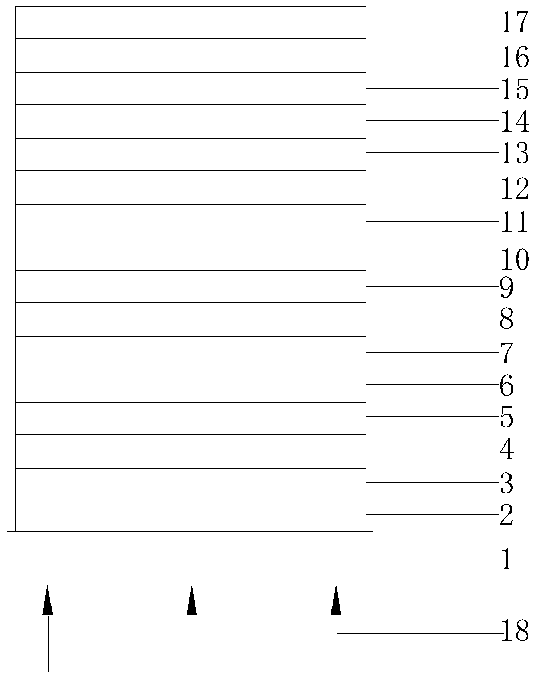
[0041] A perovskite photodetector with a vertical energy band gradient based on the charge narrowing absorption effect, comprising a glass substrate 1 coated with a first transparent conductive electrode layer 2, the first transparent conductive electrode Layer 2 is sequentially spin-coated with a first hole transport layer 3, a perovskite sensitive layer a4, and a first electron transport layer 5 from bottom to top, and the first electron transport layer 5 is sequentially coated with a first electron transport layer from bottom to top. A hole blocking layer 6, a second transparent conductive electrode layer 7, the second transparent conductive electrode layer 7 is sequentially spin-coated with a second hole transport layer 8, a perovskite sensitive layer b 9, a second electron The transport layer 10 and the second electron transport layer 10 are sequentially coated with a second hole blocking layer 11 and a third transparent conductive electrode layer 12 from bottom to top, an...
Embodiment 2
[0069] On the basis of embodiment 1, the difference between this embodiment and embodiment 1 is that the thickness of perovskite sensitive layer a, perovskite sensitive layer b and perovskite sensitive layer c is 1500nm, and a new Mixing ratios to prepare perovskite precursor solution a, perovskite precursor solution b and perovskite precursor solution c.
[0070] Dissolve methylamine lead chloride in DMF (N-N dimethylformamide) solution, and stir at 100°C for 6 hours to obtain perovskite precursor solution a; : 2 was dissolved in DMF (N-N dimethylformamide) solution, after stirring at 100°C for 6h, the perovskite precursor solution b was obtained; methylamine lead bromine was dissolved in DMF (N-N dimethylformamide) solution In , after stirring at 100°C for 6 h, the perovskite precursor solution c was obtained.
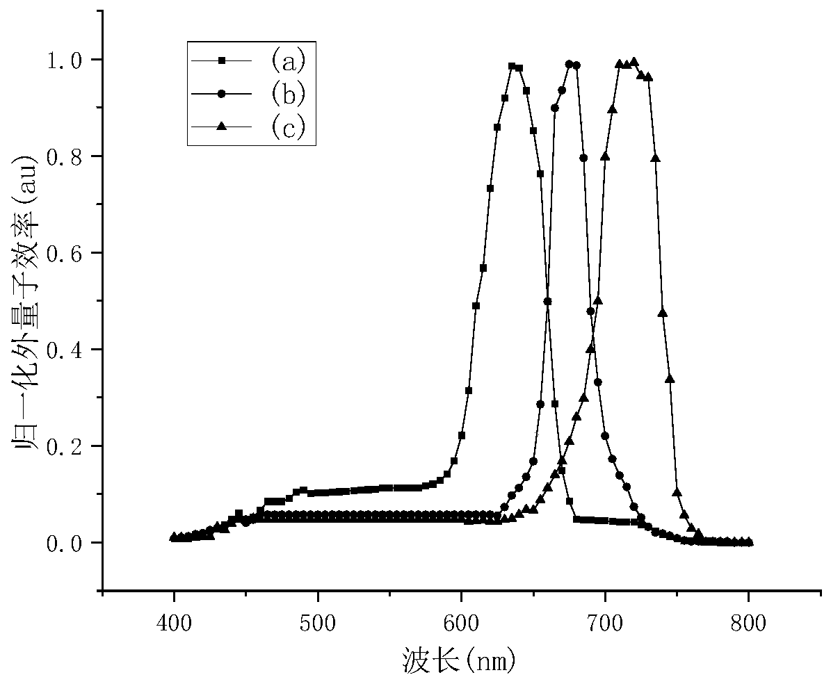
[0071] Under standard test conditions, the light beam is drawn from the light source, so that the incident light 18 is vertically incident on the perovskite photode...
Embodiment 3
[0073] On the basis of embodiment 1, the difference between this embodiment and embodiment 1 is that the thickness of perovskite sensitive layer a, perovskite sensitive layer b and perovskite sensitive layer c is 800nm, and a new Mixing ratios to prepare perovskite precursor solution a, perovskite precursor solution b and perovskite precursor solution c.
[0074] Dissolve methylamine lead iodide and methylamine lead bromide in a DMF (N-N dimethylformamide) solution at a molar ratio of 1.4:0.6, and dope with PEIE at a mass ratio of 0.33%, and stir at 100°C for 6h to obtain Perovskite precursor solution a; methylamine lead iodide and methylamine lead bromine are dissolved in DMF (N-N dimethylformamide) solution according to the molar ratio of 1:2, and doped with PEIE of 0.33% mass ratio, in After stirring at 100°C for 6 hours, the perovskite precursor solution b was obtained; methylamine lead iodide and methylamine lead bromide were dissolved in DMF (N-N dimethylformamide) solut...
PUM
| Property | Measurement | Unit |
|---|---|---|
| Thickness | aaaaa | aaaaa |
| Thickness | aaaaa | aaaaa |
| Thickness | aaaaa | aaaaa |
Abstract
Description
Claims
Application Information
 - R&D
- Intellectual Property
- Life Sciences
- Materials
- Tech Scout
- Unparalleled Data Quality
- Higher Quality Content
- 60% Fewer Hallucinations
Browse by: Latest US Patents, China's latest patents, Technical Efficacy Thesaurus, Application Domain, Technology Topic, Popular Technical Reports.
© 2025 PatSnap. All rights reserved.Legal|Privacy policy|Modern Slavery Act Transparency Statement|Sitemap|About US| Contact US: help@patsnap.com