
A method and a system for automatically cutting off laminated silk-screen printing

An automatic cutting and silk-screening technology, which is applied in special data processing applications, instruments, electrical digital data processing, etc., can solve the problems of low accuracy and low PCB design efficiency, and achieve the goal of improving efficiency, cutting efficiency and accuracy Effect

Inactive Publication Date: 2019-05-10
ZHENGZHOU YUNHAI INFORMATION TECH CO LTD
View PDF0 Cites 0 Cited by
  • Summary
  • Abstract
  • Description
  • Claims
  • Application Information

AI Technical Summary

Problems solved by technology

[0005] This application provides a method and system for automatically cutting the overlapping silk screen to solve the problems of low accuracy and low PCB design efficiency caused by manual cutting of the overlapping silk screen in the prior art

Method used


Image

  • A method and a system for automatically cutting off laminated silk-screen printing
  • A method and a system for automatically cutting off laminated silk-screen printing
  • A method and a system for automatically cutting off laminated silk-screen printing

Examples


Embodiment 1

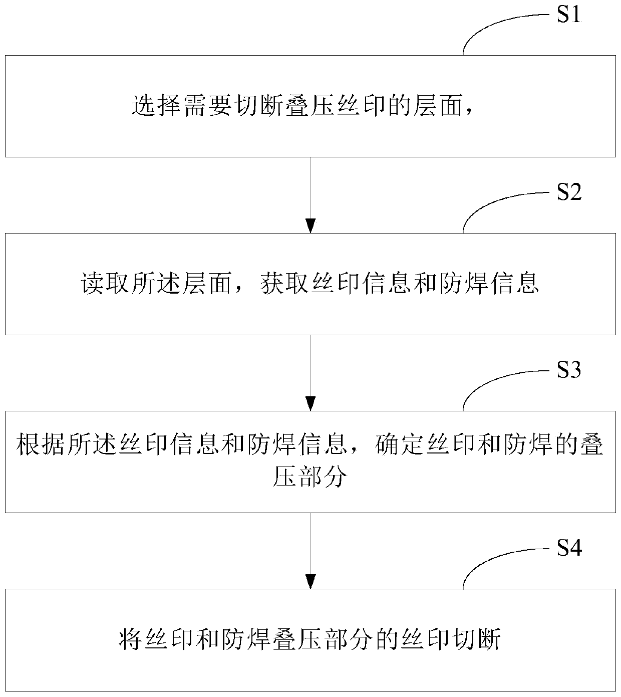
[0043] see figure 1 , figure 1 It is a schematic flow chart of a method for automatically cutting the laminated silk screen provided by the embodiment of the present application. Depend on figure 1 It can be seen that the method for automatically cutting off the laminated silk screen in this embodiment mainly includes the following process:

[0044] S1: Select the layer that needs to cut off the superimposed silk screen. Wherein, the layers in this embodiment include at least one layer of the Top silkscreen layer, the Bottom silkscreen layer, the Top solder mask layer and the Bottom solder mask layer. That is: one or more layers of Top silk screen layer, Bottom silk screen layer, Top solder mask layer and Bottom solder mask layer.

[0045] The PCB usually includes multiple layers. In this embodiment, only the silk screen layer and / or the solder mask layer related to the laminated silk screen can be selected according to the acquired command. Among them, the Top silkscreen...

Embodiment 2

[0065] exist Figure 1-Figure 3 On the basis of the illustrated embodiment see Figure 4 , Figure 4 It is a schematic structural diagram of a system for automatically cutting laminated silk screens provided in the embodiment of the present application. Depend on Figure 4 It can be seen that the system for automatically cutting the laminated silk screen in this embodiment mainly includes: a layer selection module, a silk screen information and solder mask information acquisition module, a laminated part determination module and a cutting module.

[0066] Wherein, the layer selection module is used to select the layer that needs to cut off the laminated silk screen, wherein the layer in this embodiment includes at least one layer of the Top silk screen layer, the Bottom silk screen layer, the Top solder mask layer and the Bottom solder mask layer. The silk screen information and solder mask information acquisition module is used to read the selected layer and obtain the sil...


PUM


Abstract

The invention discloses a method and system for automatically cutting off laminated silk-screen, and the method comprises the steps: selecting a layer surface which needs to cut off the laminated silk-screen, reading the selected layer surface, and obtaining silk-screen information and solder mask information; according to the silk-screen printing information and the solder mask information, determining a silk-screen printing and solder mask laminating part; and cutting off the silk screen of the silk screen and solder mask overlying part. The system for automatically cutting off the overlyingsilk screen mainly comprises a layer selection module, a silk screen information and anti-welding information acquisition module, an overlying part determination module and a cutting module. Throughthe method and the system, the screen printing and solder mask information can be accurately and rapidly acquired, the cutting efficiency and accuracy are greatly improved, and the PCB design efficiency can be improved.

Description

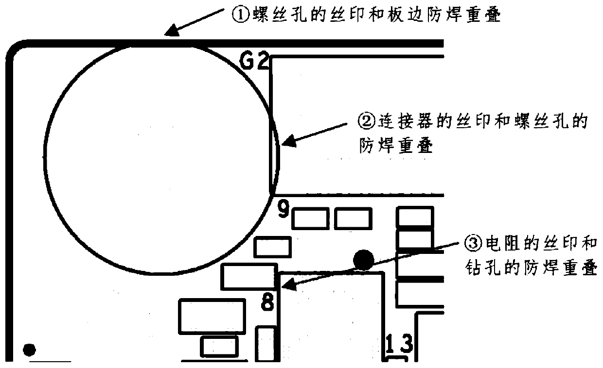
technical field [0001] The present application relates to the technical field of PCB board layout (wiring) design, in particular to a method and system for automatically cutting off laminated silk screens. Background technique [0002] In the PCB (Printed Circuit Board, printed circuit board, also known as printed circuit board) design stage of the server board, if the design scheme changes, in order to retain the reusable part of the original design, it is usually necessary to replace the unqualified part of the PCB board. The whole module of the module is intercepted from the original design in order to redesign and modify it. Since there may be components on the front or back of the PCB board, the silk screen layer and the solder mask layer in the PCB board may be overlapped. Therefore, when the unqualified module is cut from the PCB board as a whole, it is necessary to cut off the overlapped silk screen. [0003] The current method of cutting the laminated silk screen i...

Claims


Application Information

Patent Timeline
IPC IPC(8): G06F17/50
Inventor 毛晓彤
Owner ZHENGZHOU YUNHAI INFORMATION TECH CO LTD
Learn More