A high-quality semi-insulating silicon carbide single crystal and substrate doped with a small amount of vanadium

A silicon carbide single crystal, semi-insulating technology, applied in the direction of single crystal growth, single crystal growth, crystal growth, etc., can solve problems such as a large number of defects, uncontrollable crystal quality, and unstable substrate resistivity.

Active Publication Date: 2020-03-24
SICC CO LTD
View PDF5 Cites 0 Cited by
  • Summary
  • Abstract
  • Description
  • Claims
  • Application Information

AI Technical Summary

Problems solved by technology

However, the intrinsic point defect has a high migration rate in the crystal, and at a certain temperature (such as the temperature condition of GaN epitaxial layer preparation), migration, diffusion and annihilation will occur, which will cause the instability of the substrate resistivity, Also affect the stability of device performance
[0005] The vanadium concentration [V] in doped semi-insulating silicon carbide single crystal is usually 1×10 17 ~1×10 18 cm -3 , corresponding to a nitrogen concentration [N] higher than 10 17 cm -3 The high-concentration

Method used


Image

  • A high-quality semi-insulating silicon carbide single crystal and substrate doped with a small amount of vanadium
  • A high-quality semi-insulating silicon carbide single crystal and substrate doped with a small amount of vanadium
  • A high-quality semi-insulating silicon carbide single crystal and substrate doped with a small amount of vanadium

Examples


Embodiment 1

[0080] Example 1 Preparation of semi-insulating silicon carbide single crystal—impurity removal by thermal field device

[0081] The thermal field device includes graphite crucible and graphite insulation felt, and the graphite insulation felt and graphite crucible used for preparing silicon carbide single crystal are subjected to high-temperature purification. The high-temperature purification step includes: placing silicon carbide powder in the graphite crucible, the particle size of the powder is controlled at 50-500 μm, and the quantity is controlled at 50%-80% of the volume of the crucible. After the graphite crucible is placed in the graphite insulation felt and packaged in the silicon carbide crystal growth furnace, it is kept at a certain temperature and pressure for a period of time, and the thermal field device is used to remove impurities. The specific treatment temperature, pressure and time of thermal field 1#, thermal field 2#, thermal field 3#, thermal field 4# ...

Embodiment 2

[0085] Example 2 Preparation of semi-insulating silicon carbide single crystal primary product - mixing and growing crystals

[0086] Doping silicon carbide powder with vanadium element to prepare a small amount of vanadium-doped silicon carbide powder, 0.01-1g vanadium element should be placed in every 1kg reaction silicon carbide powder, the concentration of vanadium in silicon carbide powder after reaction Should be within 1 x 10 16 cm -3 ~1×10 17 cm -3 In order to achieve the content range of vanadium element in the subsequent crystal growth process.

[0087] Place a small amount of vanadium-doped silicon carbide powder in graphite crucibles of heat field 1#, heat field 2#, heat field 3#, heat field 4# and heat field 5# after the treatment in Example 1, and package them into long The crystal furnace is used for the crystal growth step. Taking thermal field 1# as an example to illustrate the crystal growth step, the specific crystal growth conditions of the crystal gro...

Embodiment 3

[0090] Example 3 Preparation of semi-insulating silicon carbide single crystal—annealing

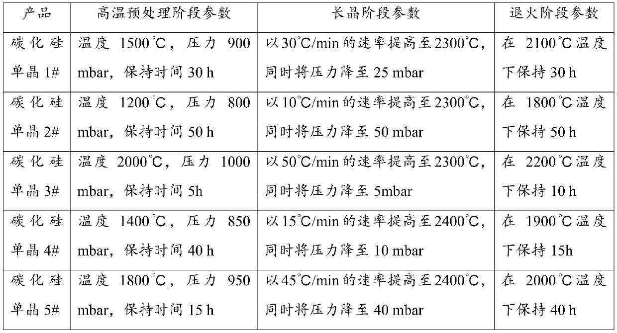
[0091] The primary silicon carbide single crystal prepared in Example 2 was further annealed to prepare a semi-insulating silicon carbide single crystal. Taking the annealing treatment of the primary silicon carbide single crystal produced by the silicon carbide single crystal growth step in the thermal field 1# as an example, the steps of preparing a silicon carbide single crystal are illustrated. The semi-insulating silicon carbide single crystal preliminary products prepared in the thermal field 1# of Example 2 respectively through the crystal growth steps in Table 2 were annealed to obtain silicon carbide single crystal 1#, silicon carbide single crystal 2#, and silicon carbide single crystal For single crystal 3#, silicon carbide single crystal 4# and silicon carbide single crystal 5#, the specific annealing conditions are shown in Table 2.

[0092] After the growth of the silicon ...


PUM


Abstract

The invention discloses high-quality semi-insulating silicon carbide single crystal doped with a small amount of vanadium and a silicon carbide single crystal substrate, and belongs to the field of semiconductor materials. The semi-insulating silicon carbide single crystal comprises shallow energy level impurities, a low-concentration deep energy level dopant and a very small amount of intrinsic point defects, wherein the shallow energy level impurities are compensated by the deep energy level dopant and the intrinsic point defects together, the concentration of the deep energy level dopant issmaller than that of the deep energy level dopant in the doped semi-insulating silicon carbide single crystal, and the concentration of the intrinsic point defects is the primary concentration of theintrinsic point defects in the silicon carbide single crystal at room temperature; and the stability of the electrical properties of the silicon carbide single crystal is not affected by the concentration of the intrinsic point defects. The semi-insulating silicon carbide single crystal has highly stable resistivity and high resistivity uniformity, and the silicon carbide single crystal substrateprepared from the silicon carbide single crystal has high resistivity uniformity and low stress, so that the silicon carbide single crystal substrate has excellent surface quality, and the stabilityand consistency of subsequent epitaxial quality are ensured.

Description

technical field [0001] The application relates to a high-quality semi-insulating silicon carbide single crystal and substrate doped with a small amount of vanadium, belonging to the field of semiconductor materials. Background technique [0002] Semi-insulating silicon carbide (SiC) single crystal substrate has become the preferred semiconductor material for GaN-based high-frequency microwave devices due to its excellent physical properties such as large band gap, high resistivity and thermal conductivity, and strong breakdown field. With the continuous development of 5G technology, the demand for semi-insulating silicon carbide single crystal substrates on the market side continues to expand. More importantly, batch commercial applications have also put forward higher quality requirements for silicon carbide semi-insulating single crystal substrates. high demands. [0003] The semi-insulating silicon carbide single crystal that has been industrialized at present is based o...

Claims


Application Information

Patent Timeline
IPC IPC(8): C30B23/02C30B29/36C30B33/02
CPCC30B23/025C30B29/36C30B33/02
Inventor 高超刘家朋李加林李长进李霞张红岩
Owner SICC CO LTD
Why Eureka
Try Eureka