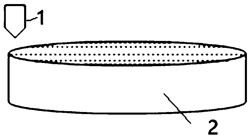
A high-purity silicon carbide single crystal substrate
A high-purity silicon carbide and silicon carbide single crystal technology, applied in the direction of single crystal growth, single crystal growth, crystal growth, etc., can solve large lattice stress, lattice distortion, increase of GaN and silicon carbide lattice fitness and other issues, to achieve the effect of improving the lattice matching degree, high quality, and high lattice fitting degree
- Summary
- Abstract
- Description
- Claims
- Application Information
AI Technical Summary
Problems solved by technology
Method used
Image

Examples
preparation example Construction
[0055] The preparation of the high-purity silicon carbide single wafer of the present application can be prepared by methods in the art, and the following preparation method of the high-purity silicon carbide single wafer can be used, which includes the following steps:
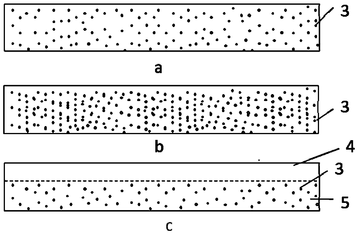
[0056] ①. Put a certain amount of silicon carbide powder in a graphite crucible. The purity of the silicon carbide powder should be above 99.9999%, and the concentration of shallow-level donor impurities such as nitrogen contained in it should be 1×10 16 cm -3 Below, the sum of the concentration of shallow-level acceptor impurities such as boron and aluminum should be 1×10 16 cm -3 the following;
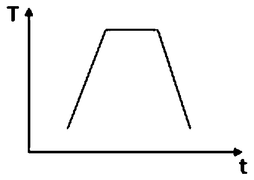
[0057] ②. After placing the seed crystal for growing silicon carbide single crystal on the upper part of the silicon carbide powder inside the graphite crucible, seal the graphite crucible; place the sealed graphite crucible inside the graphite insulation felt, and move it to single crystal growth as a whole Sea...
Embodiment 1
[0061] Example 1 Preparation of high-purity silicon carbide single crystal substrate
Embodiment approach
[0062] As an embodiment, a method for preparing a high-purity silicon carbide single wafer, the method includes the following steps:
[0063] ①. Put a certain amount of silicon carbide powder in a graphite crucible. The purity of the silicon carbide powder should be above 99.9999%, and the concentration of shallow-level donor impurities such as nitrogen contained in it should be 1×10 16 cm -3 Below, the sum of the concentration of shallow-level acceptor impurities such as boron and aluminum should be 1×10 16 cm -3 the following;
[0064] ②. After placing the seed crystal for growing silicon carbide single crystal on the upper part of the silicon carbide powder inside the graphite crucible, seal the graphite crucible; place the sealed graphite crucible inside the graphite insulation felt, and move it to single crystal growth as a whole Seal the furnace inside the equipment;
[0065] ③. Vacuumize the pressure in the furnace to 10 -5 Pa and keep it for 8 hours to remove the ...
PUM
| Property | Measurement | Unit |
|---|---|---|
| thickness | aaaaa | aaaaa |
| thickness | aaaaa | aaaaa |
| thickness | aaaaa | aaaaa |
Abstract
Description
Claims
Application Information
 - R&D
- Intellectual Property
- Life Sciences
- Materials
- Tech Scout
- Unparalleled Data Quality
- Higher Quality Content
- 60% Fewer Hallucinations
Browse by: Latest US Patents, China's latest patents, Technical Efficacy Thesaurus, Application Domain, Technology Topic, Popular Technical Reports.
© 2025 PatSnap. All rights reserved.Legal|Privacy policy|Modern Slavery Act Transparency Statement|Sitemap|About US| Contact US: help@patsnap.com