Current-type digital-analog converter output stage circuit capable of adjusting output common-mode level

A digital-to-analog converter and output stage circuit technology, applied in the direction of digital-to-analog converters, etc., can solve the problems of low common-mode voltage accuracy, difficult circuit design, affecting the working state of the load circuit, etc., to improve the power supply rejection ratio and improve the loop The effect of road gain

Active Publication Date: 2019-01-04
上海奥令科电子科技有限公司
View PDF5 Cites 4 Cited by
  • Summary
  • Abstract
  • Description
  • Claims
  • Application Information

AI Technical Summary

Problems solved by technology

Due to the circuit architecture, the output common-mode level is fixed, resulting in the output voltage range of the digital-to-analog converter being too close to the power supply voltage, which causes great difficulties for the design of subsequent circuits in the chip.
[0003] Its improved version circuit, such as figure 2 As shown, although the output common-mode voltage can be adjusted, the accuracy of the common-mode voltage is relatively low. figure 2 The variation of the resistance with the semiconductor process parameters in the architecture shown is completely independent of the variation of the transistors of the load circuit with the process parameters, and the resistance varies greatly with the process parameters (such as about + / -20% resistance value variation), resulting in Under different semiconductor process angles, the output common-mode level of the output stage circuit will be very different from the common-mode level required by the load circuit, which will affect the working state of the load circuit

Method used


Image

  • Current-type digital-analog converter output stage circuit capable of adjusting output common-mode level
  • Current-type digital-analog converter output stage circuit capable of adjusting output common-mode level
  • Current-type digital-analog converter output stage circuit capable of adjusting output common-mode level

Examples


Embodiment 1

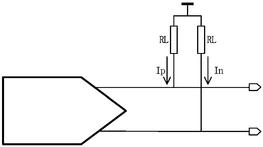
[0030] Example 1: Figure 4 It is a schematic diagram of the circuit when the output stage circuit of the present invention is connected to an independent load. The load circuit (Load Circuit) adopts a differential pair tube structure, which can represent many applications, such as amplifiers, comparators, buffers, active filters, and the like. The differential pair tube structure itself must be within a certain input common mode range to work normally, and the input reference level vcm_ref of the present invention can be generated in various ways for different applications, such as resistance voltage division, diode voltage division, current flow into Resistors, current flow into transistors, etc. are generated. Figure 4 The example in the example is that the current flows into a transistor connected to the gate and drain, and the input reference level vcm_ref generation circuit can make the non-inverting input terminal of the amplifier cmsense, that is, the output common-mo...

Embodiment 2

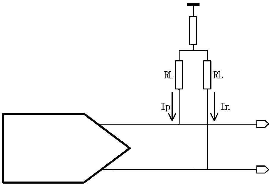
[0031] Embodiment 2: as Figure 5 , the schematic diagram of the circuit when the output stage circuit of the present invention is connected to the relevant load. At this moment, the load circuit (Load Circuit) outputs a common mode signal Vcm to indicate the common mode required by the load circuit in addition to receiving the output stage circuit output Vo_p / Vo_n level.

[0032] although Figure 4 architecture compared to figure 2 The architecture introduces a certain level of common-mode correlation to improve performance, but it still cannot meet the requirements of some applications. For example, the load circuit is a linear transconductance circuit and other applications that are sensitive to the input common-mode level. For example, the load circuit is a Application of source follower with constant output common mode, etc. At this time, the load circuit usually designs an output Vcm signal, which represents the common-mode input level required by the load circuit, a...


PUM


Abstract

The invention discloses a current-type digital-analog converter output stage circuit capable of adjusting the output common-mode level, and the circuit comprises a negative feedback loop system and adigital-analog converter. The negative feedback loop system comprises a transistor M1, a transistor M2, a load resistor RL1, a load resistor RL2 and an amplifier, wherein the joint of the load resistor RL1 and the load resistor RL2 is connected with the normal phase input terminal cmsense of the amplifier, and the other end of the load resistor RL1 is connected with the output terminal vo_p of thedigital-analog converter and the drain electrode of the transistor M1. The other end of the load resistor RL2 is connected with the output end vo_p of the digital-analog converter and the drain electrode of the transistor M2. A reference level vcm_ref is connected with the inverted input of the amplifier, and the output end amp_out of the amplifier is connected with the gate electrode of the transistor M1 and the gate electrode of the transistor M2. According to the invention, a reference common-mode level can come from a normal biasing circuit, and also can come from a load circuit, therebyachieving the perfect matching of the common-mode level between an output stage circuit and the load circuit.

Description

technical field [0001] The invention relates to the technical field of analog integrated circuits, and more specifically relates to a current conversion voltage circuit. Background technique [0002] At present, the output of the current-mode digital-to-analog converter is usually a pair of resistors, and the output current of the current-mode digital-to-analog converter flows through the resistors to generate a voltage, such as figure 1 shown. Among them, the total output current of the digital-to-analog converter is Itot=Ip+In, the output voltage is (Ip-In)*RL, and the output common-mode voltage is Vdd-(Ip+In)*RL / 2=Vdd-Itot*RL / 2 (where Vdd is the supply voltage), the output voltage ranges from Vdd to Vdd-Ttot*RL. Due to the circuit architecture, the output common-mode level is fixed, resulting in the output voltage range of the digital-to-analog converter being too close to the power supply voltage, which causes great difficulties in the design of subsequent circuits in...

Claims


Application Information

Patent Timeline
Patent Type & Authority Applications(China)
IPC IPC(8): H03M1/66
CPCH03M1/66
Inventor 王冬辉王昕宇
Owner 上海奥令科电子科技有限公司
Why Eureka
Try Eureka