Epitaxial structure and preparation method of group III nitride compound with non-polar face
A non-polar surface, epitaxial structure technology, used in semiconductor devices, electrical components, circuits, etc.
- Summary
- Abstract
- Description
- Claims
- Application Information
AI Technical Summary
Problems solved by technology
Method used
Image
Examples
preparation example Construction
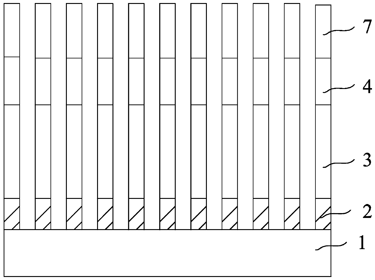
[0049] The embodiment of the present invention also provides a method for preparing a group III nitride epitaxial structure on a non-polar surface, comprising the following steps:
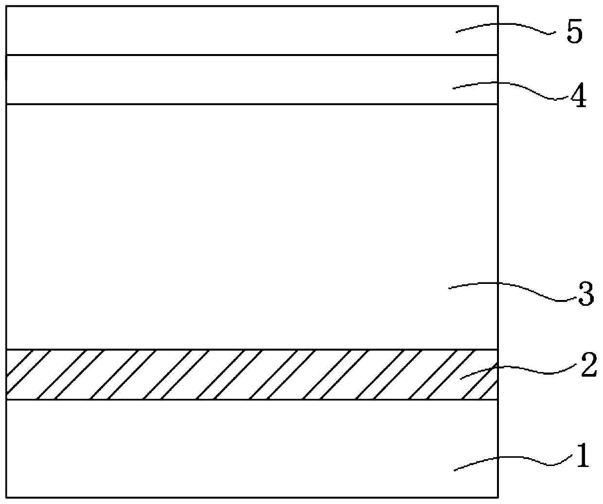
[0050] S10, growing the nucleation layer 2 epitaxially on the non-polar surface of the substrate 1;
[0051] S20, epitaxially growing a first non-polar group III nitride layer 3 on the nucleation layer 2;
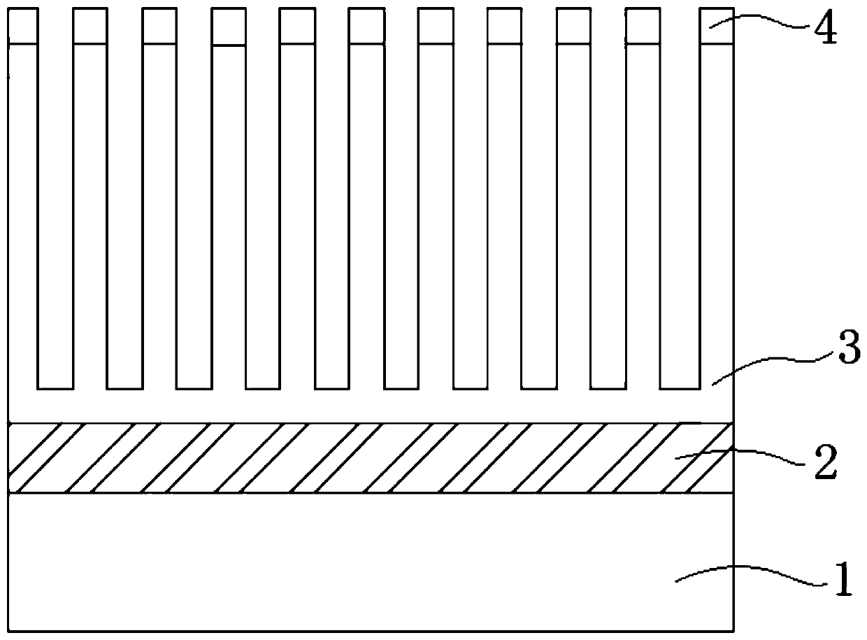
[0052] S30, covering the patterned mask layer 4 on the first non-polar group III nitride layer 3;
[0053] S40, etching down to the substrate 1 through the patterned mask layer 4 to form a plurality of primary epitaxial columnar structures spaced apart from each other; and
[0054] S50 , epitaxially growing the second non-polar group III nitride layer 7 on the surface of the patterned mask layer 4 to obtain a plurality of secondary epitaxial columnar structures spaced apart from each other. 7.
[0055] The preparation method of the present invention forms the nucleation layer 2 and the first ...
Embodiment 1
[0069] Using MOCVD in An aluminum nitride (AlN) nucleation layer 2 is grown on the r-plane sapphire substrate 1, and the thickness of the AlN nucleation layer 2 is 150 nm;
[0070] Epitaxial growth on the AlN nucleation layer 2 by MOCVD The first non-polar surface aluminum nitride layer on the non-polar surface (the first non-polar surface Group III nitride layer 3), the thickness of the first non-polar surface aluminum nitride layer is 3.5 mm;
[0071] Using PECVD to grow 300nm SiO on the first non-polar surface aluminum nitride layer 2 mask layer 4, the SiO 2 The thickness of the mask layer 4 is 80nm;
[0072] Use a coater to coat the photoresist evenly on the SiO at a speed of 4000rpm 2 A photoresist layer 5 is formed on the mask layer 4;
[0073] disposing the mask plate on the photoresist layer 5, and irradiating with ultraviolet light to remove the photoresist irradiated by ultraviolet light, and the wavelength range of ultraviolet light is 280nm-190nm;
[0074] ...
Embodiment 2
[0078] Using MBE in growing a gallium nitride nucleation layer 2 on the r-plane sapphire substrate 1, the thickness of the gallium nitride nucleation layer 2 being 40 nm;
[0079] Using MOCVD to epitaxially grow on the GaN nucleation layer 2 The first non-polar surface gallium nitride layer on the non-polar surface (the first non-polar surface Group III nitride layer 3), the thickness of the first non-polar surface gallium nitride layer is 4 mm;
[0080] Using PECVD to grow 300nm SiO on the first non-polar surface gallium nitride layer 2 mask layer 4, the SiO 2 The thickness of the mask layer 4 is 90nm;
[0081] Use a coater to coat the photoresist evenly on the SiO at a speed of 4000rpm 2 A photoresist layer 5 is formed on the mask layer 4;
[0082] disposing the mask plate on the photoresist layer 5, and irradiating with ultraviolet light to remove the photoresist irradiated by ultraviolet light, the wavelength range of ultraviolet light is 400nm-315nm;
[0083] For ...
PUM
| Property | Measurement | Unit |
|---|---|---|
| thickness | aaaaa | aaaaa |
| diameter | aaaaa | aaaaa |
| thickness | aaaaa | aaaaa |
Abstract
Description
Claims
Application Information
 - R&D
- Intellectual Property
- Life Sciences
- Materials
- Tech Scout
- Unparalleled Data Quality
- Higher Quality Content
- 60% Fewer Hallucinations
Browse by: Latest US Patents, China's latest patents, Technical Efficacy Thesaurus, Application Domain, Technology Topic, Popular Technical Reports.
© 2025 PatSnap. All rights reserved.Legal|Privacy policy|Modern Slavery Act Transparency Statement|Sitemap|About US| Contact US: help@patsnap.com


