A machine for preparing SOI silicon wafers by laser fragmentation technology
A laser slicing and silicon wafer technology, applied in semiconductor/solid-state device manufacturing, electrical components, circuits, etc., can solve the problems of low production efficiency, temperature cannot be precisely controlled and adjusted according to needs, etc., to eliminate lattice defects. Effect
- Summary
- Abstract
- Description
- Claims
- Application Information
AI Technical Summary
Problems solved by technology
Method used
Image

Examples
Embodiment 1
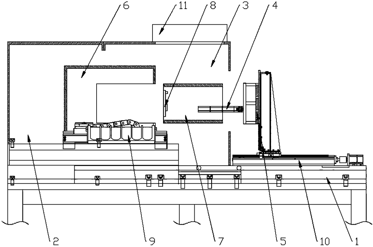
[0037] The wafer is placed on the wafer 4;
[0038] Start the slideway 10, and send the wafer 4 into the furnace tube 7 through the feeding tray 5;
[0039] The edge of the feeding tray 5 is closed with the furnace tube 7 to realize sealing;
[0040] The transmission bearing 9 drives the heat preservation pipe 6 to move to the right, and the furnace pipe 7 is embedded in the heat preservation pipe 6;
[0041] For the heat preservation pipe 6 function, the furnace pipe 7 is heated once through the heat preservation pipe 6;
[0042] The transmission bearing 9 drives the heat preservation pipe 6 to move to the left, and the heat preservation pipe 6 is separated from the furnace pipe 7;
[0043] Perform functions on the laser emitting head 8 to realize secondary heating and achieve laser splitting at high temperature;
[0044] Start the cooling device 11, and after the split operation is completed, the furnace tube 7 is cooled;
[0045] Start the slideway 10, and move the wafe...
Embodiment 2
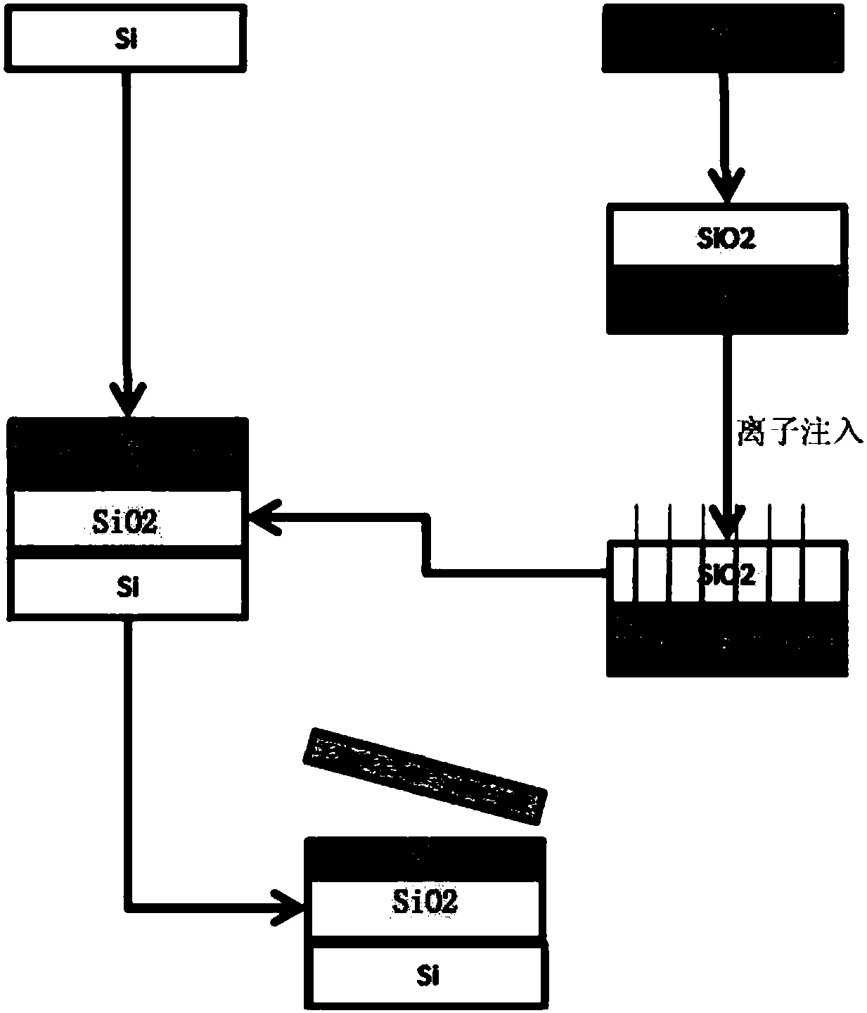
[0048] figure 2 It is a schematic diagram of the preparation of the SOI silicon wafer of the present invention, such as figure 2 As shown, take an 8-inch P-type silicon wafer, its crystal orientation can be selected from or , and the resistivity can be selected from lightly doped to high resistance.
[0049] Oxidation is carried out on one side of the silicon wafer (or both can be oxidized, according to the actual process conditions), to obtain a silicon wafer with an oxide layer (silicon dioxide is used as the BOX layer of SOI), and the oxidation adopts a conventional process, and the prepared The thickness of the oxide layer (silicon oxide) is >0-1000nm; the prepared silicon wafer with the oxide layer is cleaned with SC1 and SC2 in sequence to remove the surface pollutants of the silicon wafer, and then use the testing equipment to test the particle condition on the surface of the silicon wafer, use the testing equipment Test the thickness of silicon oxide and other para...
Embodiment 3
[0057] In Example 1, YAG laser (wavelength is 1.06 μm) is adopted, the laser spot size is 1mm, and the laser power is 50w. The laser beam scans the silicon wafer in a direction perpendicular to the surface of the silicon wafer, and the scanning path is along the diameter of the silicon wafer. direction, the scanning time is 13s, the number of times of scanning silicon wafer is 10 times (the laser scans along the diameter direction of silicon wafer at a constant speed, scanning from one end of the diameter to the other end is counted as one scan), the scanning incident angle is 45°, and the surface of silicon wafer is heated by laser The temperature rises rapidly to achieve the purpose of gathering hydrogen ions in the silicon wafer to achieve the purpose of splitting.
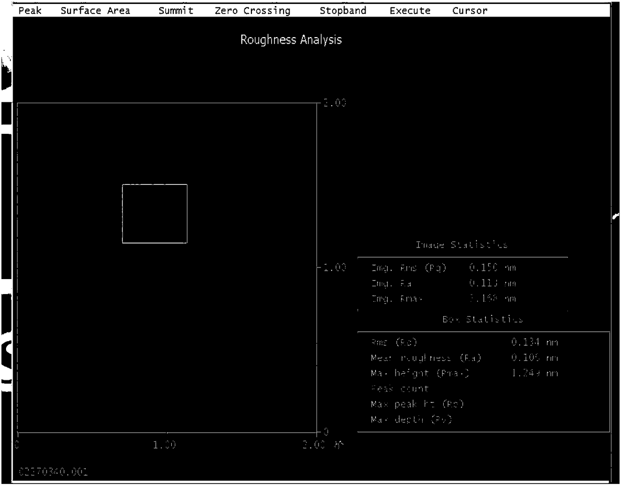
[0058] image 3 It is a schematic diagram of the SOI silicon wafer surface after the machine for preparing SOI silicon wafers by the laser splitting technology of the present invention splits; Figure 4 It is ...
PUM
| Property | Measurement | Unit |
|---|---|---|
| Thickness | aaaaa | aaaaa |
Abstract
Description
Claims
Application Information
 - Generate Ideas
- Intellectual Property
- Life Sciences
- Materials
- Tech Scout
- Unparalleled Data Quality
- Higher Quality Content
- 60% Fewer Hallucinations
Browse by: Latest US Patents, China's latest patents, Technical Efficacy Thesaurus, Application Domain, Technology Topic, Popular Technical Reports.
© 2025 PatSnap. All rights reserved.Legal|Privacy policy|Modern Slavery Act Transparency Statement|Sitemap|About US| Contact US: help@patsnap.com