A kind of large-area molecular crystal and its preparation method
A molecular crystal and large-area technology, which is applied in crystal growth, chemical instruments and methods, semiconductor/solid-state device manufacturing, etc., can solve the problems of less research and difficult preparation of organic two-dimensional semiconductors, and achieve raw material saving, good repeatability, and The effect of high uniformity
- Summary
- Abstract
- Description
- Claims
- Application Information
AI Technical Summary
Problems solved by technology
Method used
Image

Examples
Embodiment 1
[0039] Example 1, Preparation and Characterization of CMUT Monolayer Molecular Crystals
[0040] The CMUT used in this embodiment is according to the literature (Wu, Q.et al.Dicyanomethylene-Substituted Fused Tetrathienoquinoid for High-Performance, Ambient-Stable, Solution-Processable n-Channel Organic Thin-Film Transistors.Chem.Mater.23,3138-3140 (2011)) method synthesis.
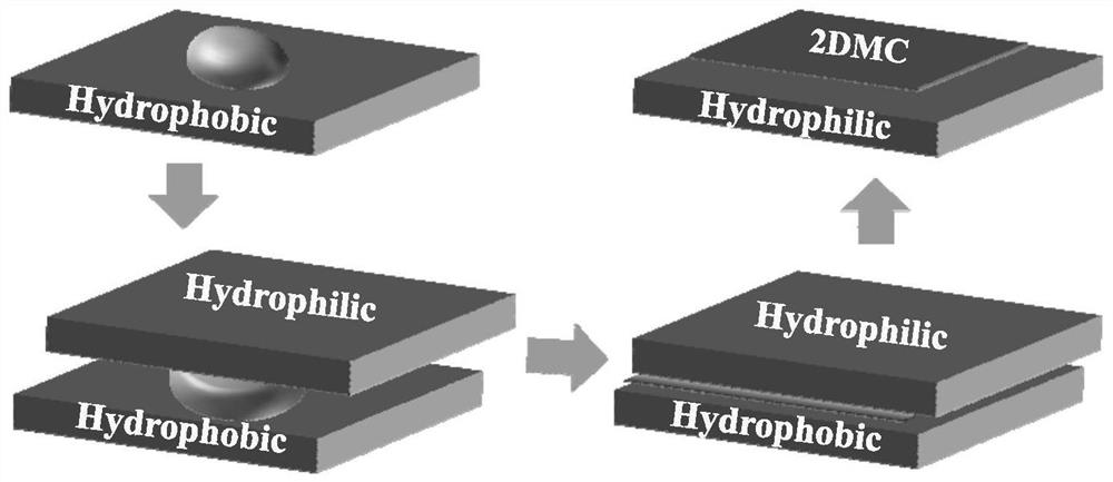
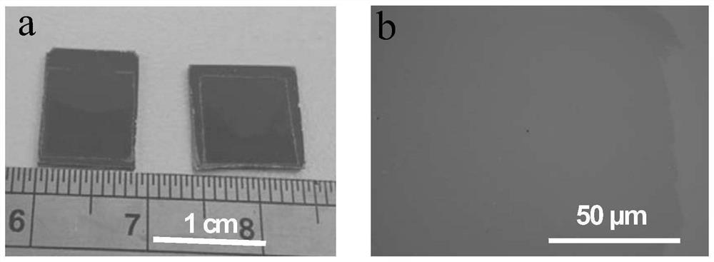
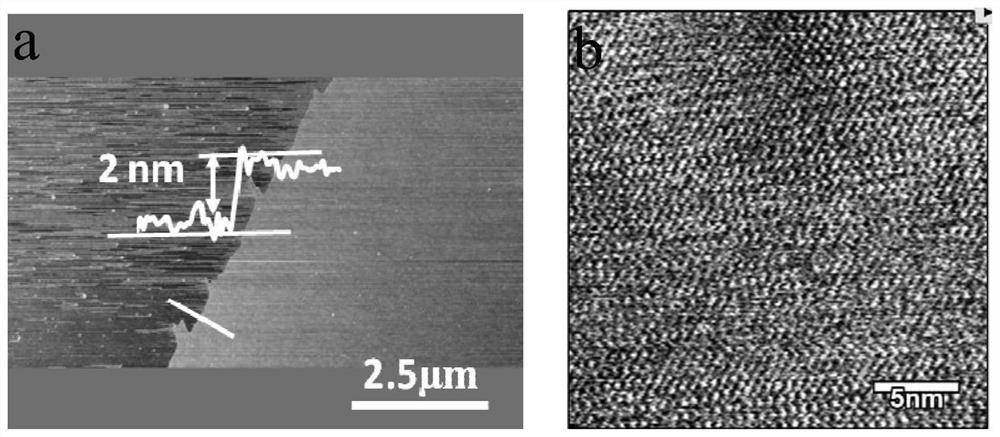
[0041] according to figure 1 As shown in the schematic diagram, a smaller-sized OTS hydrophobic substrate-modified oxide-doped silicon wafer is placed in a vessel at room temperature as a hydrophobic substrate, and an organic semiconductor with a volume concentration of 15 mg / mL is dripped on it. solution (the solvent is chlorobenzene), then cover it with an oxidation-doped silicon wafer whose size is slightly larger than that of the hydrophobic substrate as a hydrophilic substrate, and cover the vessel with a lid. After 12 hours, it was taken out, and a large-area organic semiconductor two-dimensional ...
Embodiment 2
[0045] Embodiment 2, device preparation
[0046] The CMUT organic semiconductor two-dimensional molecular crystal prepared in Example 1 was constructed into a field effect transistor by using a method of transferring a gold film by a mechanical probe.
[0047] Figure 5 a and Figure 5 b are the transfer characteristic curve and output characteristic curve of the field effect transistor with the CMUT two-dimensional molecular crystal structure, respectively. It can be seen that the mobility of the device can reach up to 2.8cm 2 V -1 the s -1 .
Embodiment 3
[0048] Example 3, Preparation and Characterization of HTEB Monolayer Molecular Crystals
[0049] The HTEB used in this embodiment is according to the literature (Meng, Q.et al.New Type of Organic Semiconductors for Field-Effect Transistors with Carbon-carbon Triple Bonds, Ambient-Stable, Solution-Processable n-Channel Organic Thin-FilmTransistors.J.Mater .Chem.19, 1477-1482 (2009)) method synthesis.
[0050] according to figure 1 As shown in the schematic diagram, a small BCB-modified oxide-doped silicon wafer is placed in a vessel at room temperature as a hydrophobic substrate, and an organic semiconductor solution with a volume concentration of 0.01 mg / mL is dripped on it. (the solvent is chlorobenzene), and then cover it with an oxidation-doped silicon wafer whose size is slightly larger than that of the hydrophobic substrate as a hydrophilic substrate, and cover the vessel lid. After 16 hours, it was taken out, and a large-area organic semiconductor two-dimensional molec...
PUM
 Abstract
Description
Claims
Application Information
 - R&D
- Intellectual Property
- Life Sciences
- Materials
- Tech Scout
- Unparalleled Data Quality
- Higher Quality Content
- 60% Fewer Hallucinations
Browse by: Latest US Patents, China's latest patents, Technical Efficacy Thesaurus, Application Domain, Technology Topic, Popular Technical Reports.
© 2025 PatSnap. All rights reserved.Legal|Privacy policy|Modern Slavery Act Transparency Statement|Sitemap|About US| Contact US: help@patsnap.com