


Quick Research
Generate reliable direction feasibility study reports for your R&D in just a few steps.

Technical Q&A
Discover and master advanced knowledge NOW. Basics, ideas, possibilities, all at once.

Find Solutions
As an expert in R&D theories, this can generate solutions to your technical problems instantly.

Evaluate Feasibility
Analyze your overall solution with one click, know your potential R&D risks in advance.

Monitor Landscape
Get weekly tech updates, stay abreast of the latest tech innovations and key insights.
Boron-doped diamond modified attenuated total reflection wafer and preparation method and application thereof
A boron-doped diamond and attenuated total reflection technology, applied in the field of attenuated total reflection wafers, can solve the problems of low catalytic activity, low electrode conductivity, narrow application range, etc., and achieve simple experimental operation, not easy to fall off, and strong repeatability Effect
- Summary
- Abstract
- Description
- Claims
- Application Information
AI Technical Summary
Problems solved by technology
Method used
Image

Examples
Embodiment 1
[0049] Steps of BDD film deposition on silicon wafer by hot wire chemical vapor phase:
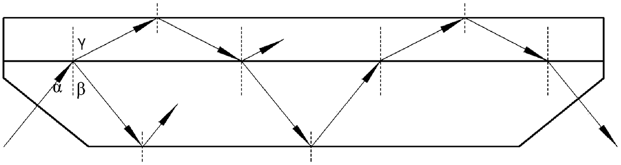
[0050] (1) Substrate pretreatment. Prepare an ATR made of Si material as the substrate, with a length of 8cm, a width of 5cm, and a height of 1cm. The infrared light can be reflected and refracted in the lower ATR in the range of incident angle 23-45°, and can be totally reflected in the upper BDD film. The surface is mechanically polished to Mirror finish. Then apply 0.1-0.5 μm diamond abrasive paste on the polished upper surface of Si and grind for 10 minutes to increase the nucleation density. Then use alcohol to ultrasonically clean for 30 minutes to remove oil stains on the surface of the substrate. In order to increase the diamond nucleation point on the crystal surface, put the cleaned sample into the acetone suspension of diamond nanopowder for ultrasonic seeding for 30 minutes, and then dry it in the air. It can leave defects and high-energy sites on the surface.
[0051] (2) ...
Embodiment 2
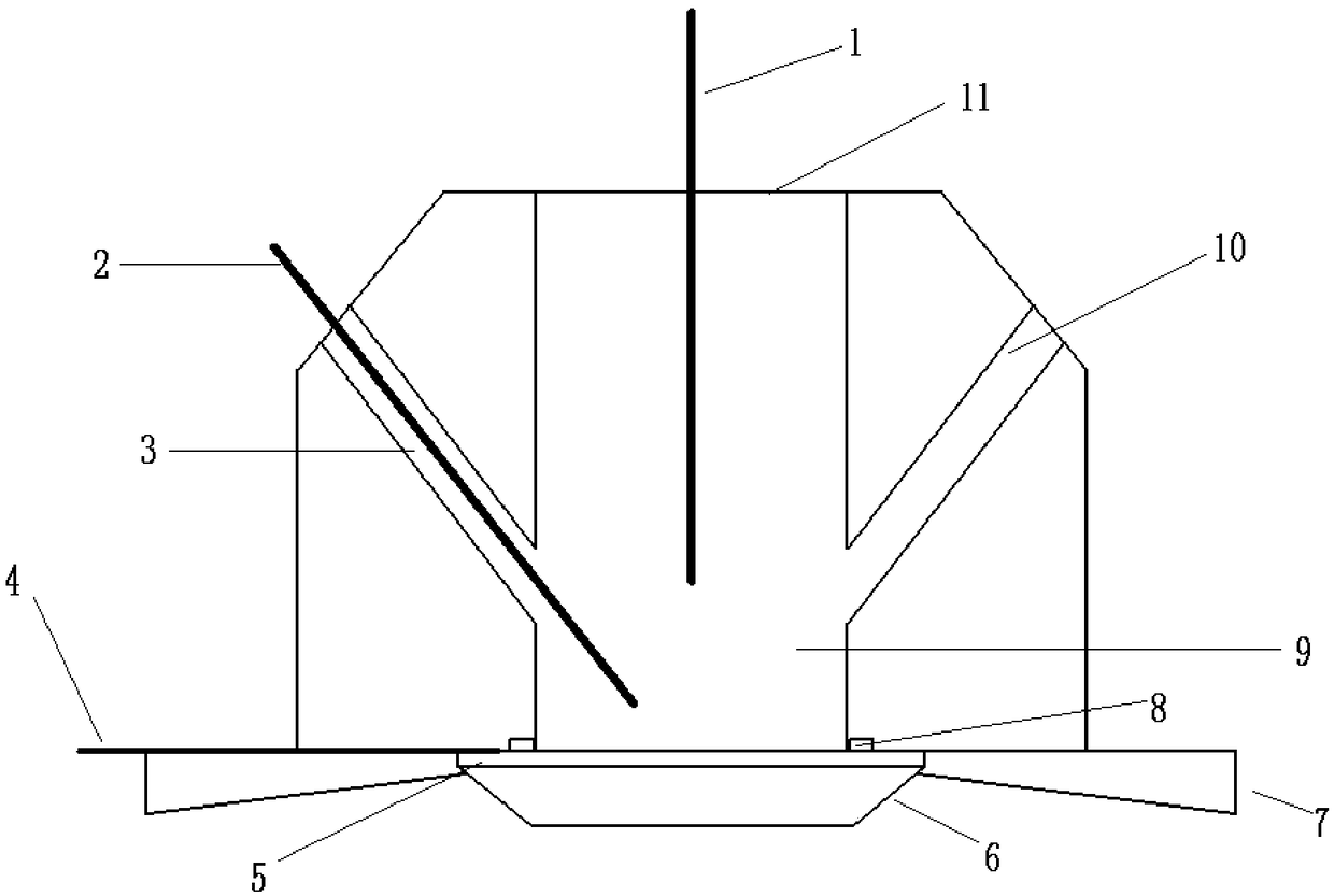
[0056] The BDD film prepared in Example 1 was used as a working electrode for electrochemical in-situ infrared spectroscopy detection: figure 2 It is one of the schematic diagrams of the cooperating use of the boron-doped diamond-modified ATR chip for infrared in-situ electrochemical detection and the electrochemical device.
[0057] (1) The BDD film 5 is used as the anode, and the working electrode of the electrochemical workstation is connected through the copper sheet 4 . The wafer of the present invention is placed in the supporting disc 7, on which an electrochemical cell 9 is installed, and the electrochemical cell and the BDD membrane are connected through a rubber ring 8 to prevent the solution in the reaction zone from flowing out. There are openings 3 and 10 on both sides of the electrochemical cell, and the central opening 1 is the main electrochemical reaction area. The opening 10 on one side is used to inject and absorb the solution, the opening 3 on the other s...
Embodiment 3
[0062] Prepare BDD loading wafer with the method of embodiment 1, obtain BDD film thickness 4.5 μm, boron doping amount is 1.8×10 19 boron atoms per cubic centimeter of BDD, and the BDD film resistivity is 10 -1 Ω·cm, surface roughness Rα is 120nm.
[0063] (1) The device diagram is as follows Figure 4 As shown, the BDD film 5 is used as a conductive carrier, and an electrode sheet coated with PAN / S (sulfur and polyacrylonitrile heat treatment product) is spread in the center as the positive electrode 12. One end of the stainless steel foil 13 is connected to the BDD film, and one section is connected to the electrochemical electrode. The workstation makes the positive electrode conductive. The upper surface of the positive electrode is covered with a thin film 15, which can effectively prevent the positive and negative electrodes from being short-circuited. The upper surface of the diaphragm covers the lithium electrode 14, which is also connected to the electrochemical w...
PUM
| Property | Measurement | Unit |
|---|---|---|
| electrical resistivity | aaaaa | aaaaa |
| thickness | aaaaa | aaaaa |
| electrical resistivity | aaaaa | aaaaa |
Abstract
Description
Claims
Application Information
 - R&D Engineer
- R&D Manager
- IP Professional
- Industry Leading Data Capabilities
- Powerful AI technology
- Patent DNA Extraction
Browse by: Latest US Patents, China's latest patents, Technical Efficacy Thesaurus, Application Domain, Technology Topic, Popular Technical Reports.
© 2024 PatSnap. All rights reserved.Legal|Privacy policy|Modern Slavery Act Transparency Statement|Sitemap|About US| Contact US: help@patsnap.com