X-ray broadband energy selection device and method for manufacturing same

A production method and energy selection technology, applied in the field of X-ray optics, can solve the problems that the unit size cannot reach the nanometer level, the number of reflections, the reflection ratios are different, and the bandpass imaging cannot be realized, and the bandpass energy range can be selected arbitrarily. , High yield and small size of micro-elements

Active Publication Date: 2018-11-23
LASER FUSION RES CENT CHINA ACAD OF ENG PHYSICS
View PDF11 Cites 2 Cited by
  • Summary
  • Abstract
  • Description
  • Claims
  • Application Information

AI Technical Summary

Problems solved by technology

The main basis for its energy selection is the absorption edge of the filter material, and it does not have a cut-off effect for high-energy X-rays other than the absorption edge.
At the same time, since the diameter of the round hole of the thick filter is about 5um, the period is about 10um, and its size is on the order of microns, the device cannot achieve bandpass imaging within ten microns
[0005] The latest research on transmission band-pass gating based on microchannel plate (MCP) shows that for soft X-rays with different incident angles and different energies, the number of reflections and reflection ratios on the inner wall of the MCP microchannel are different, resulting in X-rays passing through Different transmittance ratio after MCP
The element and the filter can realize narrow energy band gating, but due to the limitation of MCP's own manufacturing process, it is difficult to achieve flat top band pass
At present, the minimum diameter of MCP microchannels is 6um, and the cell size cannot reach the nanometer level, nor can it be used for bandpass imaging diagnosis with a single pixel size of several microns

Method used


Image

  • X-ray broadband energy selection device and method for manufacturing same
  • X-ray broadband energy selection device and method for manufacturing same
  • X-ray broadband energy selection device and method for manufacturing same

Examples


Embodiment 1

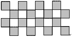
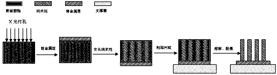
[0041] In this embodiment, the X-ray with a wavelength of less than 0.1nm on the synchrotron radiation device is used for X-ray lithography. The holes are square, the side length is 200nm, and the depth of the holes is 8um. The arrangement of the holes is as follows image 3 shown. Metal Ag with a thickness of 200 nm was plated on the surface of the perforated polycarbonate by magnetron sputtering. Then Au nanocolumns are grown in the holes on the front side of the thin metal layer 2 by electrochemical deposition until the holes are filled. On the back side of the thin metal layer 2, a polyimide support film 3 with a thickness of 2 um is pasted. Finally, the polycarbonate is dissolved by the organic solvent dichloromethane to form a nano-column array with a polyimide support film 3 .

[0042] When X-rays with a complex spectrum are irradiated on the nano-column array 1 at a grazing incidence angle of 2°, the X-rays are reflected and absorbed by the top and side walls of the ...

Embodiment 2

[0044] The embodiment of this embodiment is basically the same as that of Embodiment 1, the main difference being that the thin metal layer plated on the surface of the perforated polycarbonate by magnetron sputtering is metal Al with a thickness of 2 um. When X-rays with a complex spectrum are irradiated on the nano-column array 1 at a grazing incidence angle of 2°, the X-rays are reflected and absorbed by the top and side walls of the Au nano-columns, the thin metal layer 2 and the support film 3, and the X-ray broadband energy selection The transmittance curve of the device is as Figure 5 As shown, its gating energy band ranges from 800eV to 1600eV.

Embodiment 3

[0046] This embodiment is basically the same as that of Embodiment 1, the main difference being that the grazing incidence angle is 3.4°. When X-rays with a complex spectrum are irradiated on the nano-column array 1 at a grazing incidence angle of 3.4°, the X-rays are reflected and absorbed by the top and side walls of the Au nano-columns, the thin metal layer 2 and the support film 3, and the X-ray broadband energy selection The transmittance curve of the device is as Image 6 As shown, its gating energy band ranges from 400eV to 1400eV, including the N-band energy segment of Au. The device is placed in front of the photocathode of the framing camera, and can be used for N-band spectrum radiation framing imaging diagnosis in the gold black cavity radiation spectrum.


PUM

PropertyMeasurementUnit
Thicknessaaaaaaaaaa

Abstract

The invention provides an X-ray broadband energy selection device. The X-ray broadband energy selection device comprises a nano-rod array, a thin metal layer and a supporting film, wherein the nano-rod array is manufactured on the upper surface of the thin metal layer and the supporting film is pasted to the lower surface of the thin metal layer. The energy selection device has the advantages of small infinitesimal element size and high energy selection precision and can be applied to imaging diagnosis apparatuses with a space resolution of a few microns to realize band spectrum imaging diagnosis. The invention also provides a method for manufacturing the X-ray broadband energy selection device. The method comprises the steps of punching a polycarbonate material by using the X-ray lithography technology, and growing nano-rods in the holes by using the electrochemical deposition method to form nano-rods with great rod body perpendicularity and side wall roughness. Square nano-rod arrayswith any high aspect ratio can be manufactured according to the characteristics of to-be-selected energy sections. Band-pass energy selection in any energy section range in a soft X-ray range can berealized by flexibly design the height of the nano-rods, the material and the thickness of the thin metal layer and the grazing incident angle of X-rays.

Description

technical field [0001] The invention belongs to the fields of X-ray optics, X-spectrum diagnosis and micro-nano manufacturing, and specifically relates to an X-ray broadband energy selection device and a manufacturing method thereof. Background technique [0002] In laser indirect-driven inertial confinement fusion experiments, most of the laser energy is converted into X-rays due to the interaction between the laser and the plasma. Through the diagnosis of X-rays, many physical parameters in the interaction process can be obtained. When designing indirect-driven ICF experiments, in order to obtain high absorption efficiency and high X-ray conversion efficiency, the material of the black cavity wall is generally high-Z element gold. The high-temperature gold plasma X-ray radiation produced by laser heating the gold wall has significant non-equilibrium characteristics, that is, the X-ray spectrum has a certain band structure, usually composed of M, N, O bands and continuum. ...

Claims


Application Information

Patent Timeline
IPC IPC(8): G21B1/23B82Y20/00B82Y30/00B82Y40/00
CPCB82Y20/00B82Y30/00B82Y40/00G21B1/23Y02E30/10
Inventor 袁铮曹柱荣牛高黎宇坤邓克立王强强邓博陈韬
Owner LASER FUSION RES CENT CHINA ACAD OF ENG PHYSICS
Why Eureka
Try Eureka