


Quick Research
Generate reliable direction feasibility study reports for your R&D in just a few steps.

Technical Q&A
Discover and master advanced knowledge NOW. Basics, ideas, possibilities, all at once.

Find Solutions
As an expert in R&D theories, this can generate solutions to your technical problems instantly.

Evaluate Feasibility
Analyze your overall solution with one click, know your potential R&D risks in advance.

Monitor Landscape
Get weekly tech updates, stay abreast of the latest tech innovations and key insights.
Preparation method of ZnS infrared window antireflective microstructure surface
An infrared window and microstructure technology, applied in the field of infrared optical windows, can solve the problems of limited anti-reflection effect, instability, and difficulty, and achieve the effect of symmetrical geometric size, neat arrangement, and overcoming difficult control.
- Summary
- Abstract
- Description
- Claims
- Application Information
AI Technical Summary
Problems solved by technology
Method used
Image

Examples
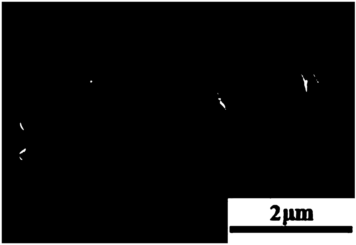
Embodiment 1
[0035] (1) ZnS substrate cleaning
[0036] The double-sided polished ZnS substrate was placed in acetone, absolute ethanol, and distilled water for ultrasonic cleaning in order to remove surface pollutants and obtain a ZnS substrate with a clean surface.
[0037] (2) Al film layer deposited on ZnS substrate
[0038] A layer of Al film was deposited on the surface of ZnS by magnetron sputtering. The sputtering process parameters are: Al target, Ar working gas, background vacuum degree better than 6×10 -4 Pa, working pressure 0.5Pa, radio frequency power 90W, argon gas flow rate 15SCCM, coating time 30min; obtain a ZnS substrate coated with an Al film, and the thickness of the Al film is 200nm.
[0039] (3) Ultrafast pulsed laser direct writing microporous structure array in Al film layer
[0040] The laser direct writing process parameters are: pulse laser power 3mW, pulse width 1ps, focusing objective lens multiple 20X, pulse repetition frequency 325Hz / s, sample stage movin...
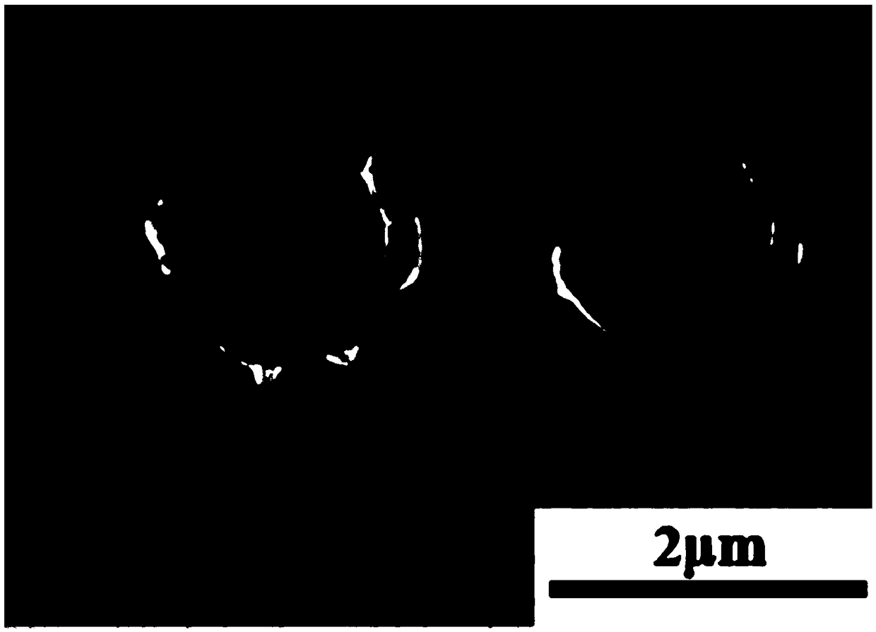
Embodiment 2
[0046] (1) ZnS substrate cleaning
[0047] The double-sided polished ZnS substrate was placed in acetone, absolute ethanol, and distilled water for ultrasonic cleaning in order to remove surface pollutants and obtain a ZnS substrate with a clean surface.
[0048] (2) Al film layer deposited on ZnS substrate
[0049] A layer of Al film was deposited on the surface of ZnS by magnetron sputtering. The sputtering process parameters are: Al target, Ar working gas, background vacuum degree better than 6×10 -4 Pa, working pressure 0.3Pa, radio frequency power 100W, argon gas flow rate 13SCCM, coating time 20min; obtain a ZnS substrate coated with an Al film, the thickness of the Al film is 150nm.
[0050] (3) Ultrafast pulsed laser direct writing microporous structure array in Al film layer
[0051] The laser direct writing process parameters are: pulse laser power 4mW, pulse width 2ps, focusing objective lens multiple 15X, pulse repetition frequency 334Hz / s, sample stage moving s...
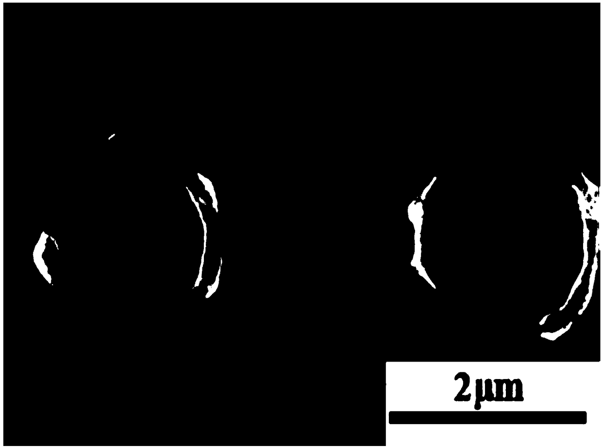
Embodiment 3
[0057] (1) ZnS substrate cleaning
[0058] The double-sided polished ZnS substrate was placed in acetone, absolute ethanol, and distilled water for ultrasonic cleaning in order to remove surface pollutants and obtain a ZnS substrate with a clean surface.
[0059] (2) Al film layer deposited on ZnS substrate
[0060] A layer of Al film was deposited on the surface of ZnS by magnetron sputtering. The sputtering process parameters are: Al target, Ar working gas, background vacuum degree better than 6×10 -4 Pa, working pressure 0.4Pa, radio frequency power 80W, argon gas flow rate 10SCCM, coating time 10min; obtain a ZnS substrate coated with an Al film, the thickness of the Al film is 100nm.
[0061] (3) Ultrafast pulsed laser direct writing microporous structure array in Al film layer
[0062] The laser direct writing process parameters are: pulse laser power 5mW, pulse width 3ps, focusing objective lens multiple 10X, pulse repetition frequency 342Hz / s, sample stage moving sp...
PUM
| Property | Measurement | Unit |
|---|---|---|
| thickness | aaaaa | aaaaa |
| thickness | aaaaa | aaaaa |
| thickness | aaaaa | aaaaa |
Abstract
Description
Claims
Application Information
 - R&D Engineer
- R&D Manager
- IP Professional
- Industry Leading Data Capabilities
- Powerful AI technology
- Patent DNA Extraction
Browse by: Latest US Patents, China's latest patents, Technical Efficacy Thesaurus, Application Domain, Technology Topic, Popular Technical Reports.
© 2024 PatSnap. All rights reserved.Legal|Privacy policy|Modern Slavery Act Transparency Statement|Sitemap|About US| Contact US: help@patsnap.com