A preparation method of black silicon substrate with ultra-low reflectivity micro-nano composite structure

A micro-nano composite structure, reflectivity technology, applied in the direction of final product manufacturing, sustainable manufacturing/processing, climate sustainability, etc., can solve the problems of low solar cell efficiency and high surface reflectivity, achieve low surface reflectivity, High repeatability and improved external quantum efficiency

Active Publication Date: 2021-05-04
HARBIN INST OF TECH
View PDF5 Cites 0 Cited by
  • Summary
  • Abstract
  • Description
  • Claims
  • Application Information

AI Technical Summary

Problems solved by technology

[0004] The invention aims to solve the problem of low solar cell efficiency due to the high surface reflectivity of existing silicon substrates, and provides a method for preparing a black silicon substrate with an ultra-low reflectivity micro-nano composite structure

Method used


Image

  • A preparation method of black silicon substrate with ultra-low reflectivity micro-nano composite structure
  • A preparation method of black silicon substrate with ultra-low reflectivity micro-nano composite structure
  • A preparation method of black silicon substrate with ultra-low reflectivity micro-nano composite structure

Examples


specific Embodiment approach 1

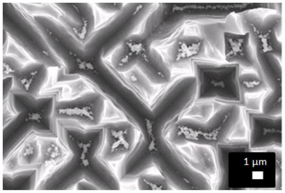
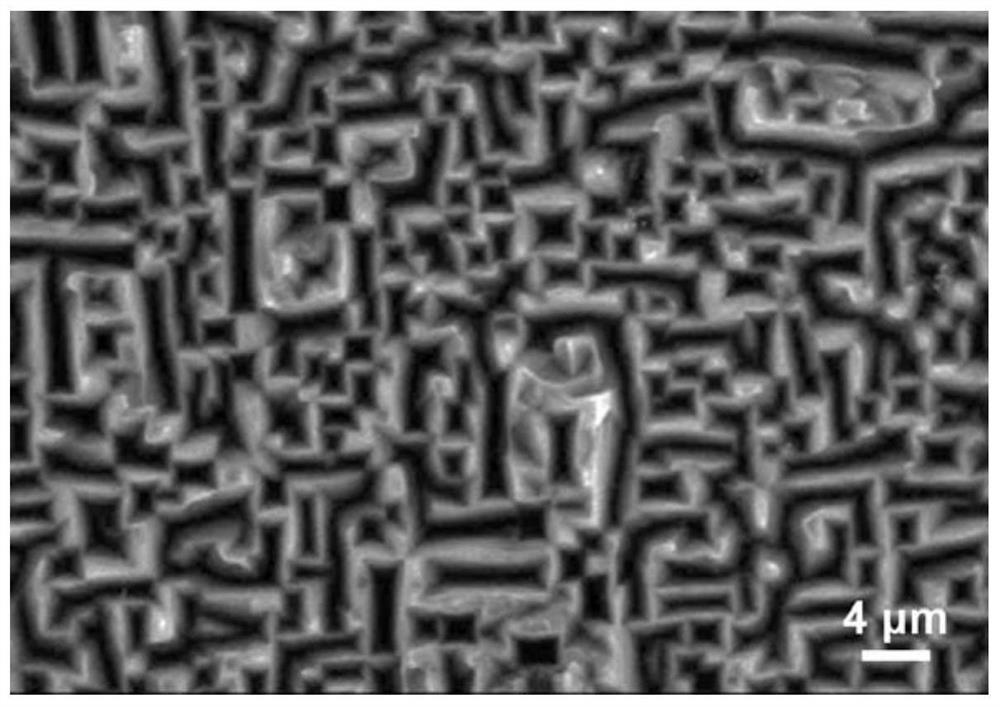
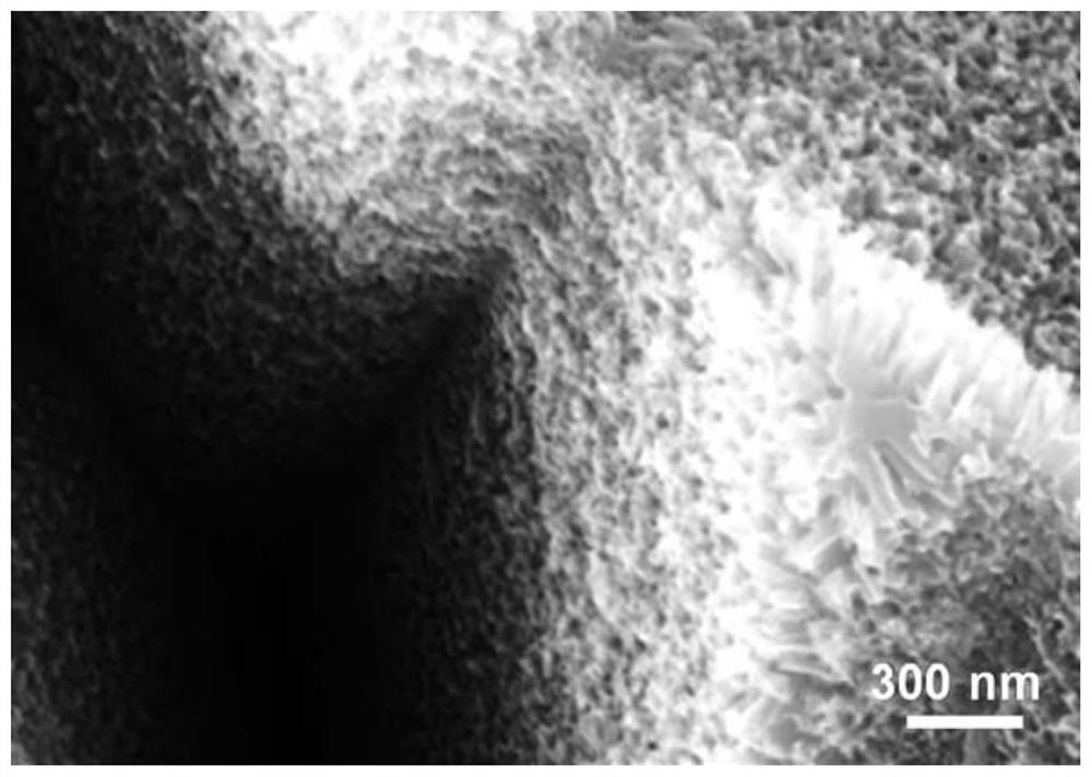
[0026] Specific Embodiment 1: In this embodiment, a method for preparing a black silicon substrate with an ultra-low reflectivity micro-nano composite structure is carried out according to the following steps:

[0027] 1. Use CuNO at a temperature of 40-100°C 3 , HF and H 2 o 2 The silicon substrate is etched with the mixed solution, and the etching time is controlled to be 1-60 minutes to obtain a silicon substrate with a micron-scale light-trapping structure on the surface;

[0028] 2. Put the silicon substrate obtained in step 1 into AgNO at a temperature of 20-100°C. 3 and HF mixed solution for the deposition of silver nanoparticles;

[0029] 3. Put the silicon substrate deposited in step 2 into HF and H at a temperature of 20-100°C. 2 o 2 In the mixed solution, etch for 10-60 minutes to obtain a silicon substrate with a micro-nano composite structure on the surface;

[0030] 4. Put the silicon substrate obtained in step 3 into HNO at a temperature of 20-100°C 3 Kee...

specific Embodiment approach 2

[0034] Specific embodiment two: the difference between this embodiment and specific embodiment one is that the CuNO described in step one 3 , HF and H 2 o 2 CuNO in mixed solution 3 The concentration of HF is 0.01~5.00mol / L, the concentration of HF is 1~10mol / L, the concentration of H 2 o 2 The concentration is 0.1~10mol / L. Others are the same as in the first embodiment.

[0035] In this embodiment, by controlling the concentration of the HF solution in step 1, the size, depth, occupation ratio and surface reflectance of the black silicon substrate of the obtained micron-scale light-trapping structure can be effectively regulated.

specific Embodiment approach 3

[0036] Embodiment 3: This embodiment differs from Embodiment 1 or Embodiment 2 in that: in step 1, the silicon substrate is (100) plane single crystal silicon. Others are the same as in the first or second embodiment.


PUM

PropertyMeasurementUnit
sizeaaaaaaaaaa
sizeaaaaaaaaaa
reflectanceaaaaaaaaaa

Abstract

A method for preparing a black silicon substrate with an ultra-low reflectivity micro-nano composite structure, the invention relates to the field of preparation of a low reflectivity black silicon substrate. The invention aims to solve the problem that the existing silicon substrate has a high surface reflectivity, resulting in low efficiency of solar cells. Method: Utilizing Cu metal catalyzed assisted chemical etching method, using CuNO 3 , HF and H 2 o 2 The mixed solution etches the silicon substrate to form a micron-scale light-trapping structure; then puts AgNO 3 The self-assembly deposition of silver nanoparticles was carried out in a mixed solution with HF; then HF and H 2 o 2 The mixed solution is subjected to Ag metal catalyzed chemical etching to complete the preparation. The invention prepares the silicon substrate with the micro-nano pattern array to realize ultra-low surface reflectivity, efficiently prepares the micro-nano pattern array structure, has high repeatability, and can control the reflectivity by optimizing the etching conditions. The black silicon substrate with ultra-low reflectivity micro-nano composite structure prepared by the invention is used in solar cells.

Description

technical field [0001] The invention relates to the field of preparation of low reflectivity black silicon substrates. Background technique [0002] As the commercial solar cell with the highest conversion efficiency and the best industrialization efficiency in the current photovoltaic market, monocrystalline silicon solar cells are widely used in aerospace, agriculture, chemical and energy fields. However, the optical loss on the surface of the silicon substrate is currently the main factor limiting the efficiency of solar cells. In order to improve the cell efficiency of solar cells, the optical loss at the surface of the silicon substrate must be reduced. At present, the methods to reduce the optical loss of the substrate surface mainly include anti-reflective coating on the surface, the use of gate electrodes and surface roughening and texturing, among which surface roughening and texturing are the most commonly used and most effective methods to reduce silicon Substra...

Claims


Application Information

Patent Timeline
Patent Type & Authority Patents(China)
IPC IPC(8): H01L31/18H01L31/0236
CPCH01L31/02366H01L31/1804Y02E10/547Y02P70/50
Inventor 张丹甘阳申健陈远东汪郑扬
Owner HARBIN INST OF TECH
Why Eureka
Try Eureka