Preparation method of flexible display screen and composite substrate for preparing flexible display screen
A flexible display and composite substrate technology, applied in semiconductor/solid-state device manufacturing, organic semiconductor devices, electric solid-state devices, etc., can solve problems such as black spots or black spots, reduce adhesion, and reduce the occurrence of black spots and black spots rate, the effect of equipment production
- Summary
- Abstract
- Description
- Claims
- Application Information
AI Technical Summary
Problems solved by technology
Method used
Image
Examples
preparation example Construction
[0037] Also, please refer to figure 2 , in another embodiment of the present invention, also proposes a kind of preparation method of flexible display screen, wherein preparation method comprises the following steps:
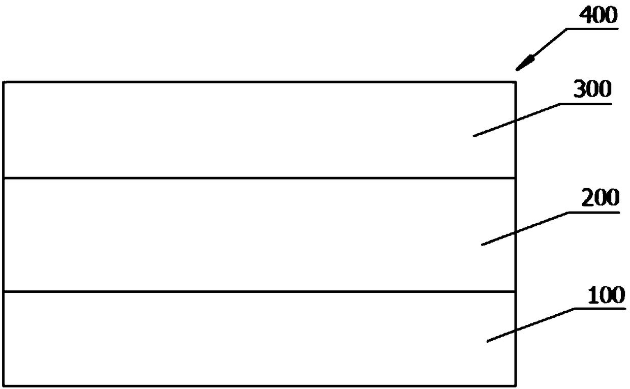
[0038] Step 500: Using a hydrogen-containing substance as a material, form a sacrificial layer 200 on the substrate 100 by chemical vapor deposition; of course, in other embodiments, this material may not be limited, and this specific method may not be limited;
[0039] In a preferred embodiment, the hydrogen-containing substance can be silane (SiH 4 ).
[0040]In a preferred embodiment, for the method of chemical vapor deposition of the sacrificial layer, it is preferable not to dehydrogenate the sacrificial layer 200 after the step of chemical vapor deposition of the sacrificial layer, so as to retain the hydrogen content in the sacrificial layer 200;
[0041] In a preferred embodiment, the hydrogen content in the sacrificial layer 200 can be adjusted by co...
Embodiment 1
[0053] A flexible display is prepared by using the composite substrate of the present invention: wherein the composite substrate includes a substrate 100 , a sacrificial layer 200 and a flexible layer 300 arranged in sequence. Wherein the substrate 100 is a glass layer (the material and thickness are the same as in Example 1), the flexible layer 300 is polyimide (the material and thickness are the same as in Example 1); the sacrificial layer 200 is prepared by a chemical vapor deposition process and has not been removed. A hydrogen-treated amorphous silicon (a-Si) layer, the thickness of the amorphous silicon (a-Si) layer being 5 nm.
[0054] After the flexible display is prepared, the substrate in the composite substrate is laser peeled off: a laser beam with a power of 19.3W is irradiated on the composite substrate from the side where the substrate 100 is located, so as to further peel off the corresponding substrate 100 and sacrificial layer 200 .
[0055] Taking 41 samples...
Embodiment 2
[0057] The composite substrate of the present invention is used to prepare a flexible display screen: wherein, the structure of the composite substrate is referred to in Embodiment 1, and the sacrificial layer 200 in the composite substrate is an amorphous silicon (a-Si) layer prepared by the same process as in Embodiment 1. The thickness of the amorphous silicon (a-Si) layer is 10 nm.
[0058] After the flexible display is prepared, the substrate in the composite substrate is laser peeled off: a laser beam with a power of 22.1 W is irradiated on the composite substrate from the side where the substrate 100 is located to further peel off the corresponding substrate 100 and sacrificial layer 200 .
[0059] Taking 45 samples as the base for testing, after laser peeling, the number of samples with black spots or black spots on the flexible display screen is 0, and the occurrence rate of black spots and black spots is 0% according to statistics.
[0060] As shown in Examples 1-2 a...
PUM
| Property | Measurement | Unit |
|---|---|---|
| Thickness | aaaaa | aaaaa |
| Thickness | aaaaa | aaaaa |
| Thickness | aaaaa | aaaaa |
Abstract
Description
Claims
Application Information
 - R&D
- Intellectual Property
- Life Sciences
- Materials
- Tech Scout
- Unparalleled Data Quality
- Higher Quality Content
- 60% Fewer Hallucinations
Browse by: Latest US Patents, China's latest patents, Technical Efficacy Thesaurus, Application Domain, Technology Topic, Popular Technical Reports.
© 2025 PatSnap. All rights reserved.Legal|Privacy policy|Modern Slavery Act Transparency Statement|Sitemap|About US| Contact US: help@patsnap.com


