High-efficiency infrared micro Fresnel lens array manufacturing method based on MEMS technology

A lens array and manufacturing method technology, applied in the field of sensors, can solve the problems of silicon-based or germanium-based mass production, low infrared transmittance of lens array resin lenses, etc., to reduce process costs and production time, improve imaging efficiency, Efficient and easy-to-control process

Active Publication Date: 2018-11-02
BESTAR HLDG +1
View PDF3 Cites 4 Cited by
  • Summary
  • Abstract
  • Description
  • Claims
  • Application Information

AI Technical Summary

Problems solved by technology

[0005] The present invention aims at the disadvantages of the conventional process of processing silicon base or germanium base that cannot mass-produce lens arrays and the shortcomings of l

Method used


Image

  • High-efficiency infrared micro Fresnel lens array manufacturing method based on MEMS technology
  • High-efficiency infrared micro Fresnel lens array manufacturing method based on MEMS technology
  • High-efficiency infrared micro Fresnel lens array manufacturing method based on MEMS technology

Examples


Embodiment Construction

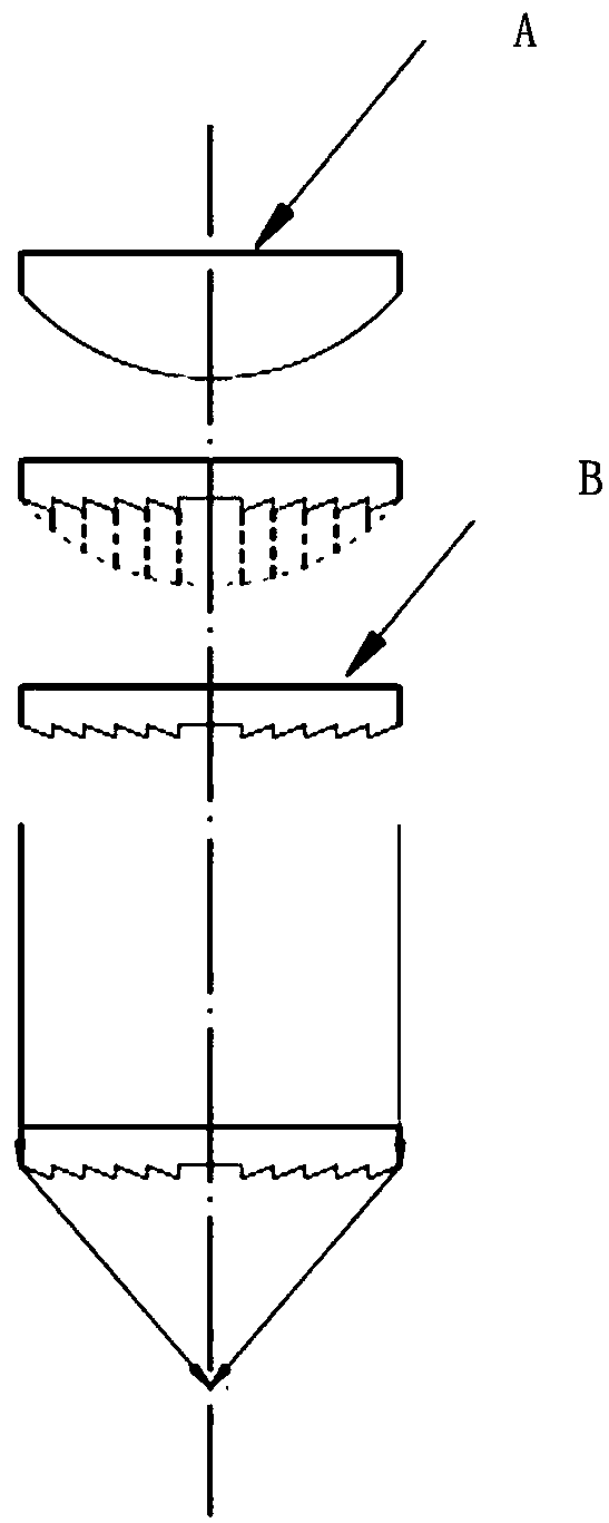
[0034] Such as Figure 6-Figure 10 A method for manufacturing an efficient infrared micro-Fresnel lens array based on MEMS technology, which includes the following MEMS process steps,

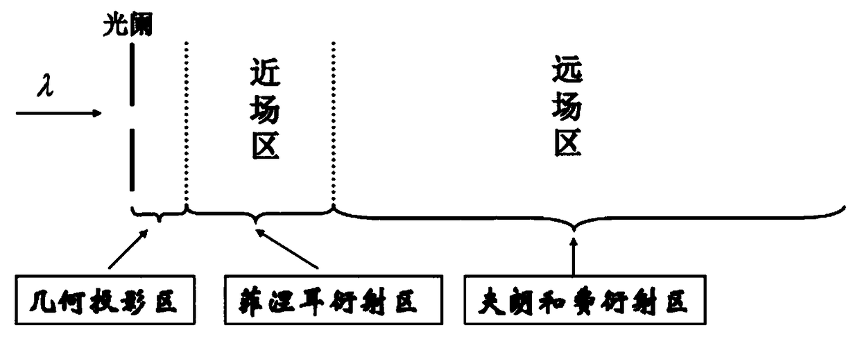
[0035] a, using the Fresnel diffraction principle to form a diffraction image;

[0036] b. The steps of making the diffraction screen: such as Figure 6 , Figure 7 As shown, several light-transmitting small hole array patterns are set on the photolithography plate or metal plate 2, and the radius of the small hole 1 is L 0 And it is arranged on the upper surface of the light-transmitting quartz plate 3 to form a diffraction screen, and the metal plate can be a chromium metal plate;

[0037] c. The step of making the receiving screen: coating a positive photosensitive photoresist 4 on the surface of the silicon wafer as the substrate 5 to form a receiving screen, and the distance between the receiving screen and the diffraction screen is z;

[0038] d, the step of exposure forming photoresi...


PUM


Abstract

The invention belongs to the field of a sensor, and particularly to a high-efficiency infrared micro Fresnel lens manufacturing method based on MEMS technology. The high-efficiency infrared micro Fresnel lens manufacturing method based on the MEMS technology comprises the following steps of forming a diffraction image by means of a Fresnel diffraction principle, manufacturing a diffraction screen,manufacturing a receiving screen, performing exposure for forming a photoresist pattern, etching a Si circular plate, and performing cleaning. According to the method of the invention, through controlling a diffraction imaging distance, a traditional lithography machine is used for directly performing diffraction exposure on a wafer surface which requires forming of the Fresnel lens array, thereby forming a Fresnel waveband plate pattern; then micro machining is performed on the developed wafer through an MEMS process facility, and finally a Fresnel lens with a preset focal length is formed on the wafer surface. The high-efficiency infrared micro Fresnel lens manufacturing method has advantages of realizing simple, high-efficiency and easy-controlling integral process, greatly reducing process cost and production time consumed in various polishing steps of a traditional silicon lens, and improving imaging efficiency.

Description

technical field [0001] The invention belongs to the field of sensors, in particular to a method for manufacturing an efficient infrared micro-Fresnel lens array based on MEMS technology. Background technique [0002] Since the British physicist William Herschel discovered infrared in 1800, he has opened up a broad road for human beings to apply infrared technology. Among many infrared technologies, infrared thermal imaging technology has quickly become the direction and focus of research and development in various countries around the world. Infrared thermal imaging technology is to detect the infrared rays radiated by each part of the scene itself, and use the difference in the radiation of each part of the scene itself to obtain the details of the image. Its essence is a wavelength conversion technology, that is, to convert the infrared radiation image into a visible image. At the same time, it is determined by the infrared transmission properties of the atmosphere and th...

Claims


Application Information

Patent Timeline
IPC IPC(8): G02B3/00G02B3/08
Inventor 王焕焕徐金国费跃
Owner BESTAR HLDG
Why Eureka
Try Eureka