A method for in-situ luminous flux monitoring and exposure dose compensation

A technology of exposure dose and compensation method, which is applied in microlithography exposure equipment, photolithography exposure device, optics, etc., can solve problems affecting luminous flux, optical element deformation, luminous flux change, etc., to improve device performance and uniform nanostructure Effect

Active Publication Date: 2020-04-17
SHANGHAI INST OF APPLIED PHYSICS - CHINESE ACAD OF SCI
View PDF4 Cites 0 Cited by
  • Summary
  • Abstract
  • Description
  • Claims
  • Application Information

AI Technical Summary

Problems solved by technology

If the exposure dose (exposure dose=luminous flux*exposure time) between each region is different during the exposure process, the nanostructure between each region will be uneven, resulting in the inhomogeneity of the nanostructure in the finally obtained large-area pattern, After this pattern is developed into a device, the performance of the device will be affected
[0006] In the actual exposure process, the luminous flux is often difficult to keep constant for a long time, which is caused by many reasons: First, although Shanghai Light Source is now operating in constant current mode, the electron beam current in the storage ring is not constant change, but after continuous attenuation and re-injection, the change of the beam current of the storage ring will affect the luminous flux; secondly, there are multiple insert devices installed in the storage ring, and the change of the gap between the inserts will affect the electron orbit, causing the electron orbit to drift. In particular, the change of the gap between the upstream and downstream inserts adjacent to the lithography beamline has the greatest impact on the lithography beamline. The drift of the electron orbit will cause the change of the light source point, which will affect the luminous flux; finally, the thermal effect of the optical elements in the beamline The impact produces deformation, which also causes a change in luminous flux

Method used


Image

  • A method for in-situ luminous flux monitoring and exposure dose compensation
  • A method for in-situ luminous flux monitoring and exposure dose compensation
  • A method for in-situ luminous flux monitoring and exposure dose compensation

Examples


Embodiment Construction

[0024] The preferred embodiments of the present invention will be given below in conjunction with the drawings and described in detail.

[0025] The present invention, namely an in-situ luminous flux monitoring and exposure dose compensation method, includes the following steps:

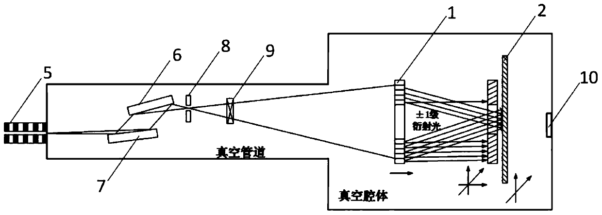
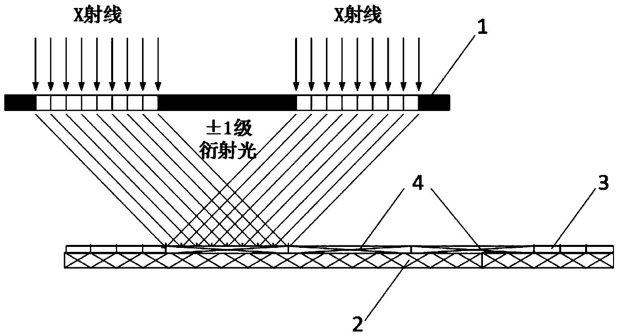
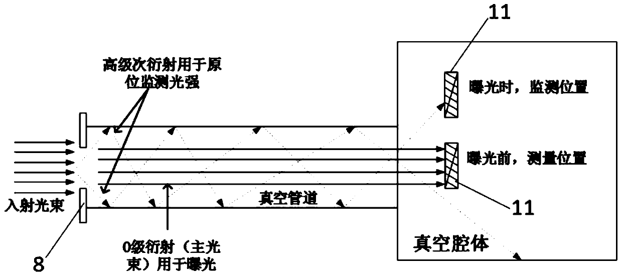
[0026] Step S1, using the existing synchrotron X-ray large area interference lithography system (such as figure 1 (Shown) Before performing the X-ray interference lithography experiment, first, adjust the incident beam (ie, X-ray) to make its intensity uniformly distributed on the mask grating 1, and set a photodiode 11 upstream of the mask grating 1 in the vacuum chamber. And make it outside the main optical path generated by the incident beam (such as image 3 As shown, the photodiode 11 is in the monitoring position at this time), the first photocurrent is measured by an ammeter (not shown) connected to the photodiode 11, and then the first luminous flux Fsu is calculated (the luminous flux calculation...


PUM


Abstract

The invention relates to an in-situ luminous flux monitoring and exposure dose compensating method. The method comprises the following steps: measuring the luminous flux of a main light beam going through an exit slit and entering a vacuum chamber before a lithography experiment by using a photodiode, monitoring the intensity of main light beam going through the exit slit and entering the vacuum chamber and the luminous flux of stray lights directly proportional to the main light beam during experimental exposure, and adjusting the exposure time of each lithographic area in real time accordingto the change of the intensity of the stray lights to compensate for the exposure dose in order to keep the exposure dose constant in the XIL large-area exposure pattern splicing process, ensure thatthe nanostructure in the finally obtained large-area exposure pattern is uniform and effectively improve the performances of a device formed by the exposure pattern.

Description

Technical field [0001] The invention relates to an in-situ luminous flux monitoring and exposure dose compensation method. Background technique [0002] X-ray interference lithography (XIL) is a new advanced micro- and nano-processing technology that uses the interference fringes of two or more coherent X-beams to expose photoresist. It can carry out nanostructure processing of tens or even a dozen nanometer cycles . XIL technology is suitable for the preparation of large-area nano-periodic structures with a period of less than 100nm. Compared with other methods such as photolithography, it can obtain high-quality sub-50nm high-density periodic nanostructures more reliably. It is used in nanoelectronics, micro-nano There are a wide range of applications in the fields of optics, nanobiology, nanodevices and materials, and photonic crystals. [0003] For a single exposure, the area of ​​the exposed pattern obtained by the XIL technology is related to the area of ​​the mask grating....

Claims


Application Information

Patent Timeline
Patent Type & Authority Patents(China)
IPC IPC(8): G03F7/20
CPCG03F7/70408G03F7/70558
Inventor 薛超凡胡纯刘平吴衍青王连升杨树敏赵俊郑丽芳邰仁忠
Owner SHANGHAI INST OF APPLIED PHYSICS - CHINESE ACAD OF SCI
Why Eureka
Try Eureka