A method to suppress the low dose rate enhancement effect of bipolar transistors
A bipolar transistor and enhancement effect technology, which is applied in bipolar transistor testing, single semiconductor device testing, etc., can solve the problems of electronic device performance degradation, increase the recombination rate of transistors, and change carriers, so as to improve the radiation resistance , Inhibition of low dose rate damage, inhibition of damage enhancement effects
- Summary
- Abstract
- Description
- Claims
- Application Information
AI Technical Summary
Problems solved by technology
Method used
Image
Examples
specific Embodiment approach 1
[0018] Embodiment 1: The method for suppressing the low dose rate effect of bipolar transistors in this embodiment, such as Figure 5 shown, including:
[0019] Step 1, put the transistor into an airtight container, and evacuate or fill with protective gas; the transistor is a bipolar transistor.
[0020] Step 2: heating the transistor with an electric furnace and keeping it warm; the heating rate is less than or equal to 20°C / min, the temperature control accuracy is ±1°C, and the heating temperature is 150°C to 300°C.
[0021] Step 3, after the heat preservation is completed, the temperature of the transistor is lowered to 25°C.
[0022] The purpose of this embodiment is to find a method for suppressing the enhancement effect of low-dose-rate radiation damage on bipolar transistors, by heating the transistors before irradiation to reduce the impact of irradiation on the space charge region of the transistors. Therefore, the phenomenon of enhanced radiation damage of transis...
specific Embodiment approach 2
[0027] Specific embodiment 2: The difference between this embodiment and specific embodiment 1 is that after the completion of step 3, it also includes a step for detecting whether there is an enhancement effect of radiation damage, specifically including:
[0028] Step four, make 60 Coγ-rays are used as an irradiation source to perform an ionizing irradiation test on the transistor, changing the irradiation dose rate and recording the change in current gain of the transistor. If the change exceeds a preset threshold, it means that the transistor is damaged.
[0029] Other steps and parameters are the same as those in Embodiment 1.
specific Embodiment approach 3
[0030] Embodiment 3: This embodiment differs from Embodiment 1 or Embodiment 2 in that the method for suppressing the low dose rate effect of bipolar transistors also includes:
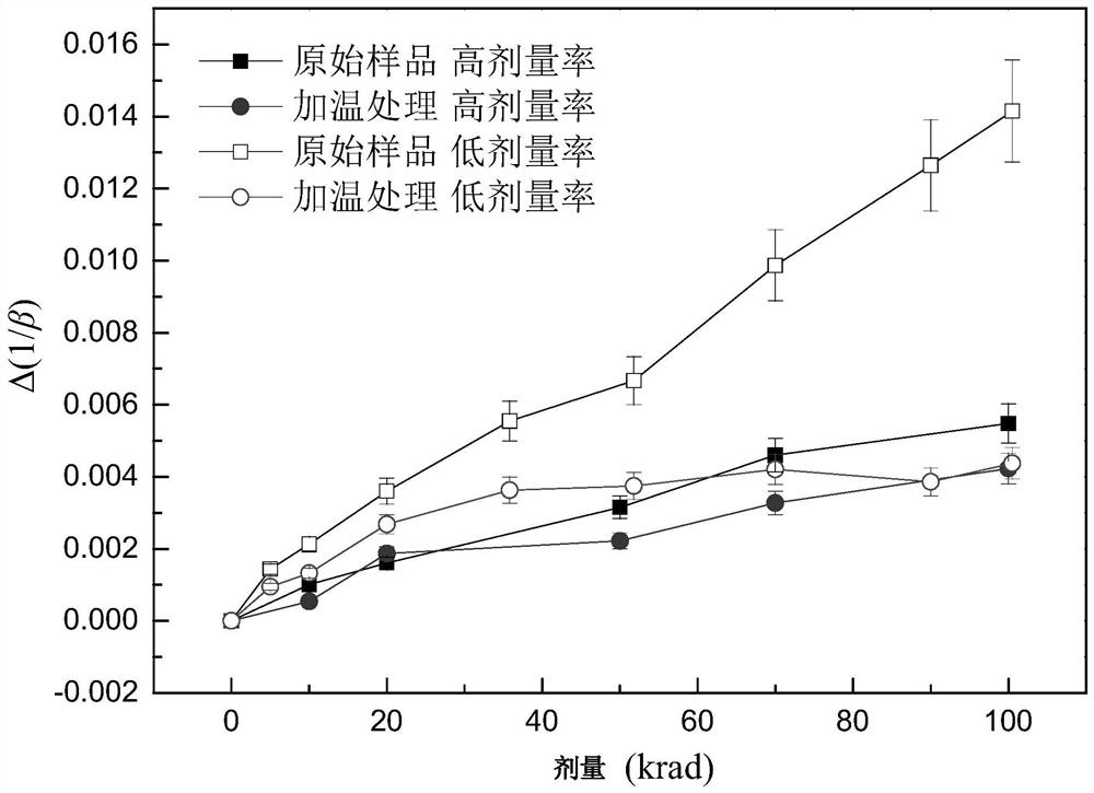
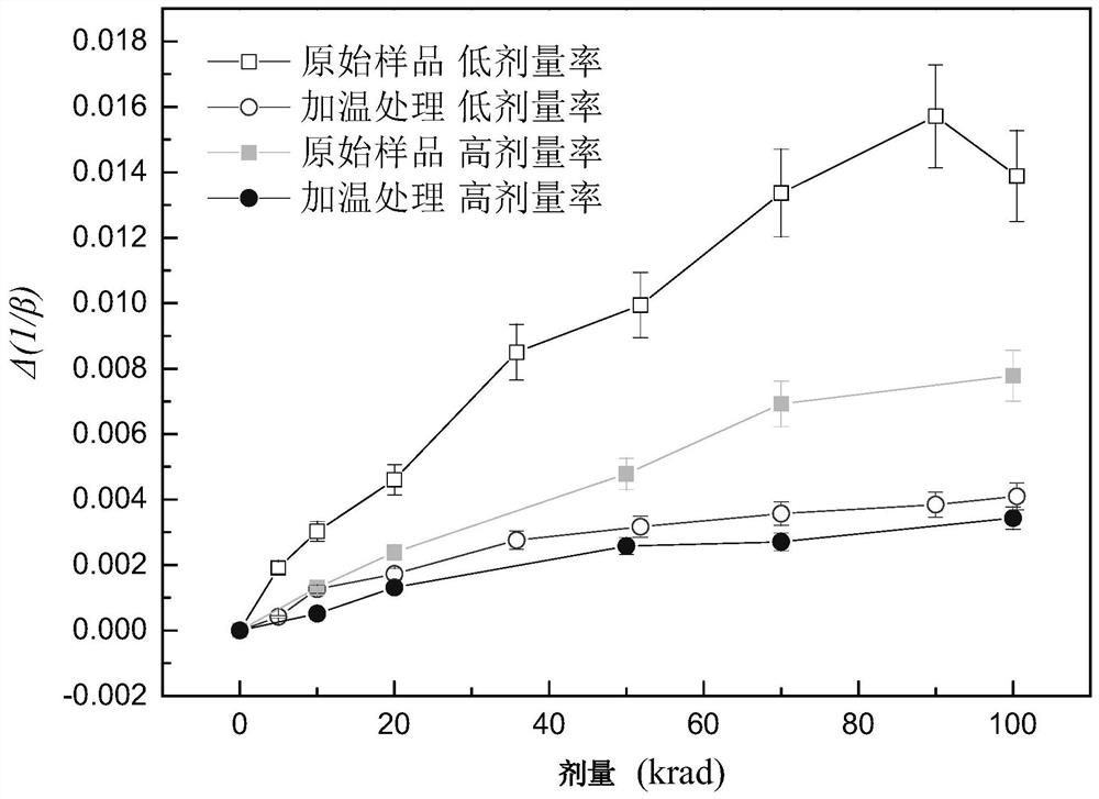
[0031] Step A, before the execution of step one, draw the graph of Δ(1 / β) versus irradiation dose for the high and low dose rate irradiation of the transistor without heating treatment; step B, after step four is executed , to plot the curves of Δ(1 / β) versus irradiation dose for high and low dose rate irradiation of transistors after heating treatment; where Δ(1 / β) represents the variation of the reciprocal of current gain.
[0032] The purpose of step A and step B is to observe the effect of irradiation on the electrical property damage of the transistor before and after heating through the drawn curve.
[0033] Methods of suppressing the low dose rate effects of bipolar transistors may also include:
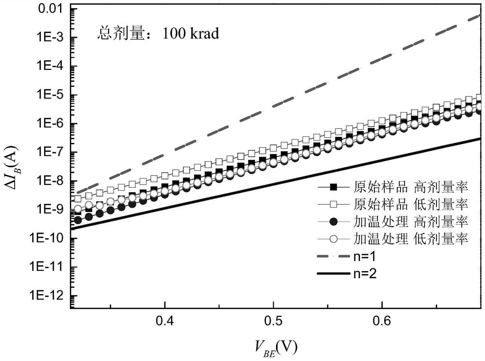
[0034] Step C. Before step 1 is executed, draw the ΔI of high and low dose rate irradiation of th...
PUM
 Abstract
Description
Claims
Application Information
 - R&D
- Intellectual Property
- Life Sciences
- Materials
- Tech Scout
- Unparalleled Data Quality
- Higher Quality Content
- 60% Fewer Hallucinations
Browse by: Latest US Patents, China's latest patents, Technical Efficacy Thesaurus, Application Domain, Technology Topic, Popular Technical Reports.
© 2025 PatSnap. All rights reserved.Legal|Privacy policy|Modern Slavery Act Transparency Statement|Sitemap|About US| Contact US: help@patsnap.com


