
A Displacement Damage-Based Method for Suppressing the Formation of Oxide Trapped Charges

A technology of displacement damage and oxide, applied in the direction of circuits, measuring electronics, electrical components, etc., can solve the problems of affecting the lifetime of minority carriers, changing the surface recombination rate of carriers, and degrading the performance of electronic devices, so as to achieve easy operation, reduce costs, Effects in simple steps

Active Publication Date: 2020-06-09
HARBIN INST OF TECH
View PDF8 Cites 0 Cited by
  • Summary
  • Abstract
  • Description
  • Claims
  • Application Information

AI Technical Summary

Problems solved by technology

Oxide trapping charges and interface states will change the surface recombination rate of carriers, thereby affecting the minority carrier lifetime, leading to degradation of the performance of electronic devices

Method used

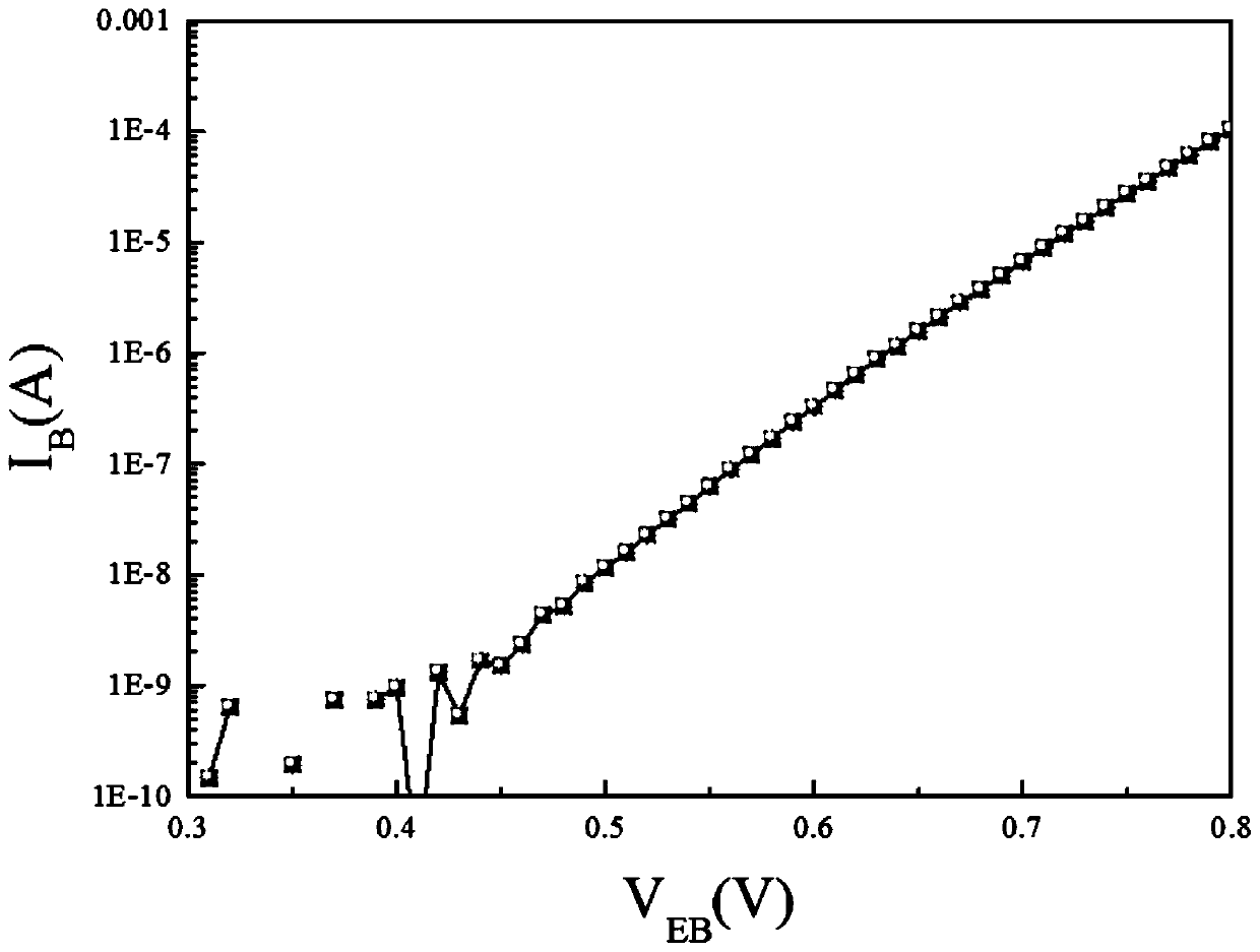
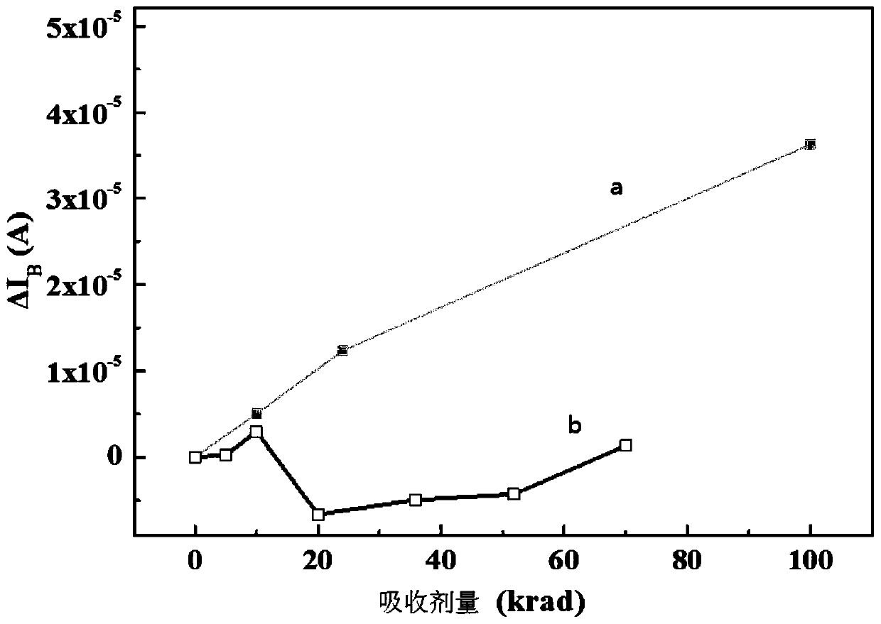
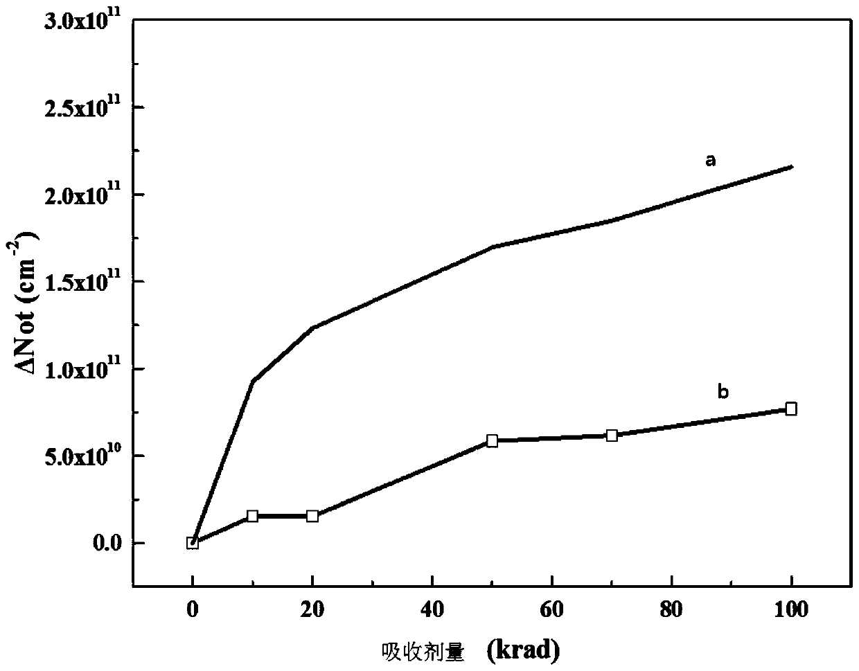

Image

  • A Displacement Damage-Based Method for Suppressing the Formation of Oxide Trapped Charges
  • A Displacement Damage-Based Method for Suppressing the Formation of Oxide Trapped Charges
  • A Displacement Damage-Based Method for Suppressing the Formation of Oxide Trapped Charges

Examples


specific Embodiment approach 1

[0025] Specific Embodiment 1: In this embodiment, a method for suppressing the formation of oxide-trapped charges based on displacement damage is carried out in the following steps:

[0026] Step 1. Determine that the farthest distance between the passivation layer and the surface in the electronic component sample is b, and the shortest distance between the passivation layer and the surface in the electronic component sample is c;

[0027] Step 2. Select the type of pre-irradiation incident particles and the energy of pre-irradiation incident particles, and calculate the incident depth t of pre-irradiation incident particles in the electronic device sample through Geant4 software 1 ;where b>t 1 > c;

[0028] Step 3, through the Geant4 software, according to the energy of the pre-irradiation incident particles selected in step 2, calculate the ionization absorbed dose I of the pre-irradiation incident particles of the unit fluence in the sample of step 1 d1 and the displaced...

specific Embodiment approach 2

[0035] Specific embodiment 2: The difference between this embodiment and specific embodiment 1 is that in step 1, the sample of electronic components adopts SiO 2 Bipolar process electronic components as insulating material and passivation layer. Others are the same as in the first embodiment.

specific Embodiment approach 3

[0036] Embodiment 3: This embodiment differs from Embodiment 1 or Embodiment 2 in that: the type of pre-irradiation incident particles in step 2 is electrons, protons, heavy ions, neutrons, photons or mesons. Others are the same as in the first or second embodiment.


PUM


Abstract

A method for inhibiting the formation of oxide trapped charges based on displacement damage is provided. The invention relates to the field of space environmental effects, nuclear science and appliedtechnology, and solves the radiation damage performance of electronic devices by oxide trapped positive charges and an interface state. The method comprises determining the farthest distance b and theclosest distance c from a passivation layer in an electronic component to the surface; calculating the range t1 of a pre-irradiated incident particle; calculating the ionizing absorbed dose Id1 and the displacement absorbed dose Dd1 of the incident particle in the passivation layer; calculating the value of Log[(Id+Dd) / Dd]; perofrming pre-irradiation and determining the irradiation injection amount [phi]1; calculating the incident depth t2 of an ionizing radiation incident particle; calculating the ionizing absorbed dose Id2 and the displacement absorbed dose Dd2 of the incident particle in the passivation layer; calculating the value of log[(Id2+Dd2) / Dd2];and perform ionizing irradiation. The method changes the inherent displacement defect state in a sample, inhibits the formation of oxide trapped positive charges, and is simple in steps and easy to operate. The method is applied to the research of space environmental effects of electronic components and the anti-radiation reinforcement technology.

Description

technical field [0001] The invention relates to the formation and evolution mechanism of ionizing radiation defects, and belongs to the field of space environment effects, nuclear science and application technology. Background technique [0002] With the development of science and technology, my country's aerospace industry has made great progress and has become one of the aerospace powers. All kinds of spacecraft are closely related to our life and safety. Electronic components used in spacecraft will inevitably be affected by the space environment during their in-orbit service. These factors include solar cosmic ray particles, galactic cosmic ray particles, and radiation environments such as the Earth's radiation belts. Electronic components play a vital role in the electronic control system and information system of a spacecraft. Various radiation environments in space will lead to its performance degradation, abnormal function and even failure. [0003] Space charged r...

Claims


Application Information

Patent Timeline
Patent Type & Authority Patents(China)
IPC IPC(8): G01R31/00H01L21/265
CPCG01R31/001H01L21/265
Inventor 李兴冀陈伟杨剑群刘超铭郭晓强王晨辉
Owner HARBIN INST OF TECH
Learn More