
a kind of mnwo 4 Nanoplate photosensitive field effect transistor and manufacturing method thereof

A field effect transistor and nanoplate technology, applied in nanotechnology, nanotechnology, final product manufacturing, etc., can solve the problems of unfavorable industrial application, low light responsivity, slow response time, etc., and achieve excellent gate control capability, Effects of high optical responsivity and specific detectivity, small threshold voltage

Active Publication Date: 2019-08-16
INST OF METAL RESEARCH - CHINESE ACAD OF SCI
View PDF2 Cites 0 Cited by
  • Summary
  • Abstract
  • Description
  • Claims
  • Application Information

AI Technical Summary

Problems solved by technology

However, due to the current large-scale preparation of 1D MnWO with high crystalline quality 4 There are still many difficulties in nanomaterials, based on 1D MnWO 4 High-performance photosensitive field-effect transistors of nanomaterials have not been reported yet
Moreover, the existing photosensitive field effect transistors based on 1D nanomaterials generally have problems such as low photoresponsivity, slow response time, and high threshold voltage, which are not conducive to industrial applications.

Method used


Image

  • a kind of mnwo  <sub>4</sub> Nanoplate photosensitive field effect transistor and manufacturing method thereof
  • a kind of mnwo  <sub>4</sub> Nanoplate photosensitive field effect transistor and manufacturing method thereof
  • a kind of mnwo  <sub>4</sub> Nanoplate photosensitive field effect transistor and manufacturing method thereof

Examples


Embodiment

[0045] In this example, MnWO 4 A method for manufacturing a nanoplate photosensitive field effect transistor, the specific steps are as follows:

[0046] 1) Will be used to grow MnWO 4 The commercial Ti sheet substrate of the nanoplate was polished with sandpaper (2000 mesh) to remove impurities and oxide layers on the surface. Then, the polished Ti sheet was ultrasonically cleaned in acetone, alcohol, and deionized water in sequence, each step was cleaned for 10 minutes to remove organic matter and ion impurities on the surface, and then dried with nitrogen gas for later use.

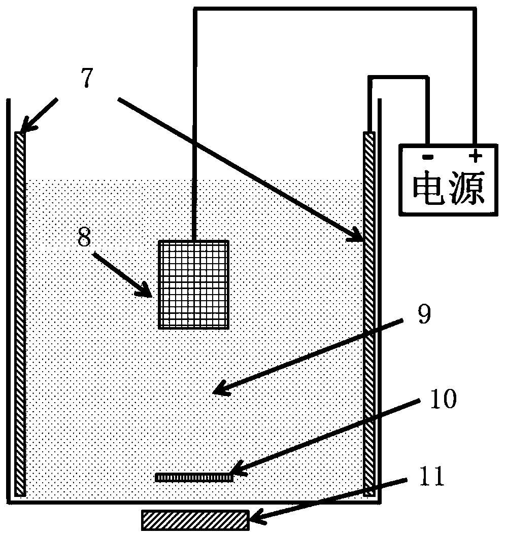
[0047] 2) Prepare a layer containing Mn on the Ti sheet in the electrolyte by using the micro-arc oxidation method. 2+ and W 6+ Ionic porous TiO 2 thin film, porous TiO 2 The porosity of the film is ~37%, the average pore size is 1 μm, and the porous TiO 2 The thickness of the film is ~20 μm. First, equip with 0.8mol / L Na 3 PO 4 12H 2 O, 0.04mol / L Na 2 B 4 o 7 10H 2 O, 0.02mol / L Na 2 WO ...


PUM


Abstract

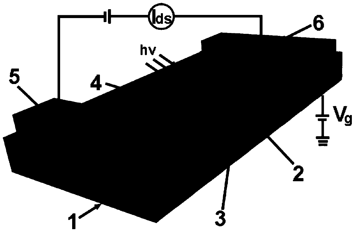
The invention belongs to the inorganic semiconductor nanomaterial technology and device application field, and especially relates to a MnWO4 nano-plate photosensitive field-effect transistor and a manufacturing method thereof. The MnWO4 nano-plate photosensitive field-effect transistor comprises a grid metal electrode, Si substrate and a SiO2 insulation layer in sequence from the bottom up. The upper surface of the SiO2 insulation layer is provided with a single MnWO4 nano-plate, a source metal electrode and a drain metal electrode. The source metal electrode and the drain metal electrode arecovered on the two ends of the single MnWO4 nano-plate respectively and form ohmic contact. The method produces the MnWO4 nano-plate having large area, high yield and excellent crystal quality througha micro-arc oxidation method; and furthermore, the MnWO4 nano-plate is utilized to prepare the MnWO4 nano-plate photosensitive field-effect transistor in a back-gate structure. The method is simple in process, is low in cost, can grow the MnWO4 nano-plate material having high crystal quality on a large scale, and facilitates industrial promotion.

Description

technical field [0001] The invention belongs to the field of inorganic semiconductor nanomaterial technology and device application, in particular to a MnWO 4 Nanoplate photosensitive field effect transistor and its manufacturing method. Background technique [0002] Field-effect transistors (TFTs) are voltage-controlled devices that control the ability of solid materials to conduct electricity by varying an electric field. Field-effect transistors are widely used in large-scale integrated circuits and display panels, and are the basis of analog and digital integrated circuits. They have the advantages of high integration, large input impedance, stable performance, and mature manufacturing processes. In 1951, Shockley first proposed the concept of a photosensitive field effect transistor, combining the light-induced effect of a semiconductor with the field effect of a transistor to make it have a photodetection function. Compared with photodiodes, photosensitive field effe...

Claims


Application Information

Patent Timeline
Patent Type & Authority Patents(China)
IPC IPC(8): H01L31/113H01L31/032H01L31/18B82Y30/00
CPCB82Y30/00H01L31/032H01L31/1136H01L31/18Y02P70/50
Inventor 刘宝丹张兴来姜亚南刘鲁生杨文进李晶姜辛
Owner INST OF METAL RESEARCH - CHINESE ACAD OF SCI
Learn More