Reception device and method, transmission device and method, and communication system

A technology for receiving equipment and transmitting equipment, applied in the fields of receiving equipment and methods, transmitting equipment and methods, and communication systems, can solve the problems of high noise interference level, signal waveform distortion, limited feasible frequency band limitation, etc. Effect

Inactive Publication Date: 2018-06-08
SONY CORP
View PDF9 Cites 0 Cited by
  • Summary
  • Abstract
  • Description
  • Claims
  • Application Information

AI Technical Summary

Problems solved by technology

[0006] However, despite the installation of wideband and lowband filters, this is limited to feasible frequency band limitations
This is because frequency band limitation simultaneously distorts the signal waveform, causes inter-symbol interference, and causes code transmission errors
[0007] On the other hand, there is a high probability that the noise spectrum will also be included in the signal frequency band
Specifically, in the case where the existing electric field communication system is installed in a digital device such as a multifunction mobile phone, since the LCD display and other digital circuits of the multifunction mobile phone are extremely close, the LCD display and other digital circuits The interference level of the noise generated in the system is very high and has a great influence on the quality of the electric field communication

Method used


Image

  • Reception device and method, transmission device and method, and communication system
  • Reception device and method, transmission device and method, and communication system
  • Reception device and method, transmission device and method, and communication system

Examples


Embodiment Construction

[0045] Hereinafter, modes for carrying out the present disclosure (hereinafter referred to as “embodiments”) will be described.

[0046]

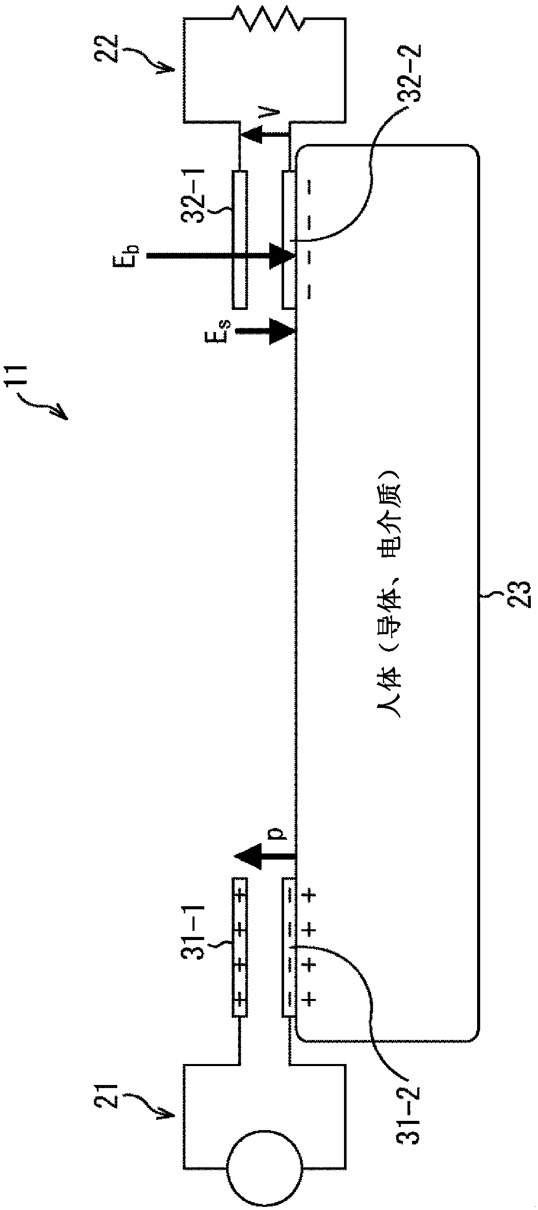
[0047] figure 1 is a diagram showing a schematic configuration example of an electric field communication system.

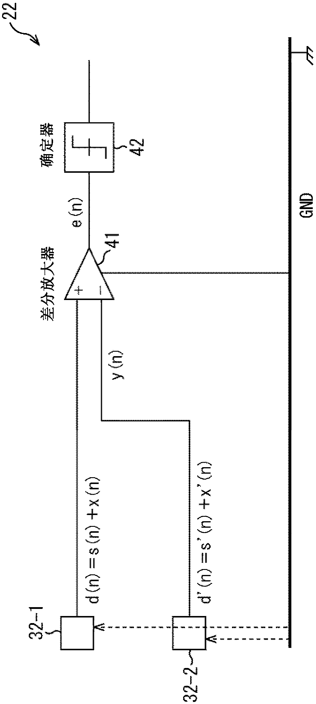
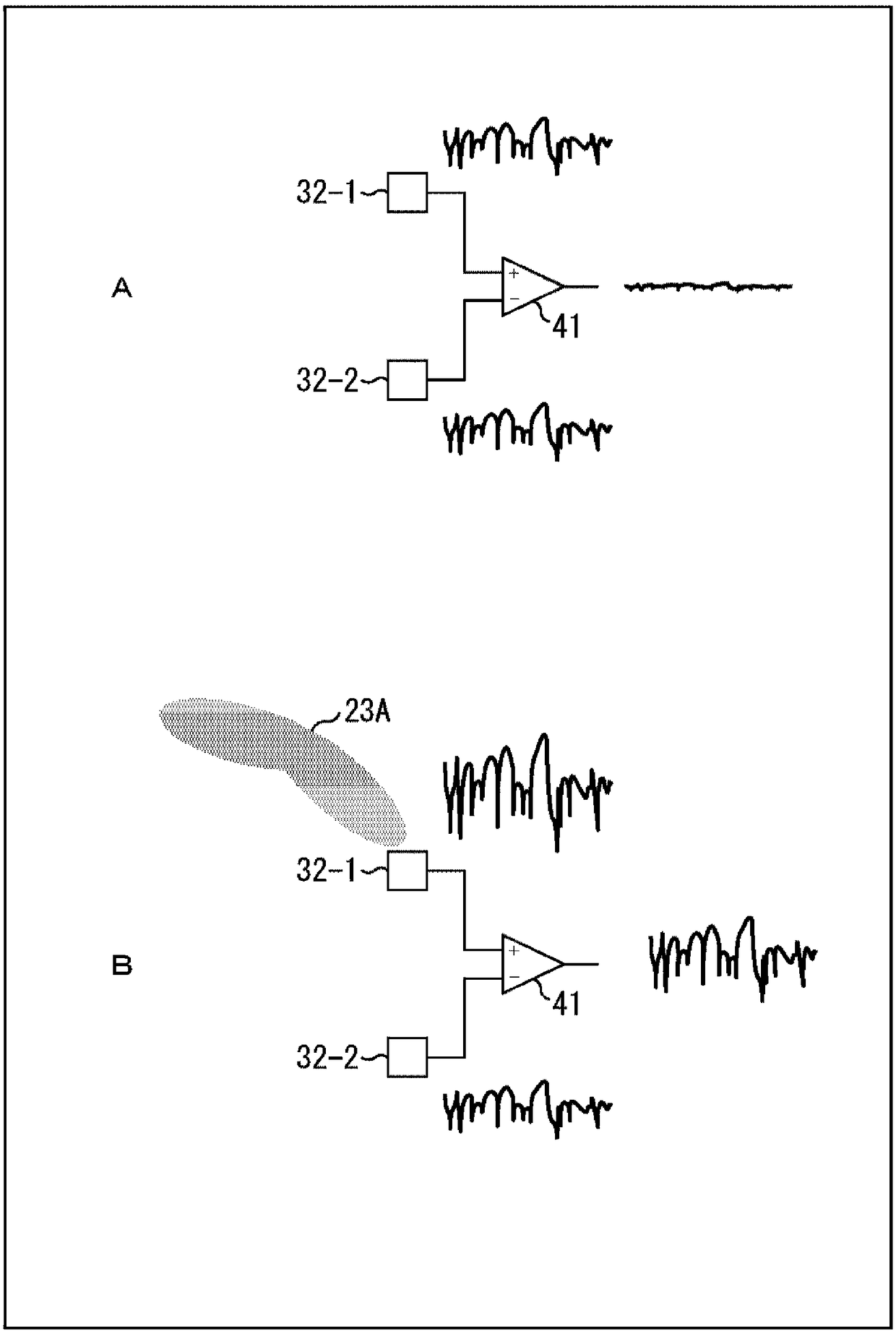
[0048] exist figure 1 In an example, the electric field communication system 11 includes a sending device 21 , a receiving device 22 , and a human body 23 . The transmitting device 21 includes a pair of two-electrode transmitting electrodes 31-1 and 31-2. The receiving device 22 includes a pair of two-electrode receiving electrodes 32-1 and 32-2. exist figure 1 In an example, the human body 23 acts as a conductor or dielectric.

[0049] Electric field communication is a communication scheme using changes in an electric field, which is different from wireless communication using electromagnetic waves. like figure 1 As shown, the transmitting device 21 causes the peripheral electric field to change by causing the voltag...


PUM


Abstract

The present disclosure relates to a reception device and method, a transmission device and method, and a communication system, with which pulse-like noise can be reduced. A signal x(n) from one reception electrode is input to a variable gain amplifier and an amplitude control circuit. The variable gain amplifier amplifies the signal x(n) from the one reception electrode and outputs an amplified signal y(n) to a differential amplifier. Upon receiving an input of a signal d(n) from the other of the reception electrodes and the signal y(n) from the variable gain amplifier, the differential amplifier outputs a differential signal e(n). By using the signal x(n) from the one reception electrode and an amplitude of the output signal from the differential amplifier, the amplitude control circuit controls an input amplitude in accordance with an algorithm for setting a gain w(n) of the variable gain amplifier. The present disclosure can be applied, for example, to an electric-field communication in which communication is performed by means of changes in the ambient electric field when air or a human body is used as a transmission medium.

Description

technical field [0001] The present disclosure relates to a receiving device and method, a transmitting device and method, and a communication system, and more particularly, to a receiving device and method, a transmitting device and method, and a communication system capable of reducing impulse noise. Background technique [0002] Electric field communication is a communication scheme using changes in an electric field, which is different from wireless communication using electromagnetic waves. As disclosed in Patent Document 1, the transmitter causes the peripheral electric field to change by causing the voltage to be applied to the transmitting electrodes to change according to the data desired to be transmitted, and the receiver detects its peripheral field from the potential difference change occurring between the receiving electrodes. Changes in the electric field and estimate the transmitted data. [0003] As standardized standards of this communication scheme, there ...

Claims


Application Information

Patent Timeline
Patent Type & Authority Applications(China)
IPC IPC(8): H04B13/00H04B1/10H04B5/02H04B15/00
CPCH04B5/02H04B15/00H04B13/005H04B1/10H04B13/00
Inventor 宇野雅博田中胜之近藤史隆田中正幸
Owner SONY CORP
Why Eureka
Try Eureka