


Quick Research
Generate reliable direction feasibility study reports for your R&D in just a few steps.

Technical Q&A
Discover and master advanced knowledge NOW. Basics, ideas, possibilities, all at once.

Find Solutions
As an expert in R&D theories, this can generate solutions to your technical problems instantly.

Evaluate Feasibility
Analyze your overall solution with one click, know your potential R&D risks in advance.

Monitor Landscape
Get weekly tech updates, stay abreast of the latest tech innovations and key insights.
Preparation method of electroless nickel immersion gold for printed circuit board
An electroless immersion nickel gold and printed circuit board technology, which is applied in the manufacturing of printed circuits, the formation of printed circuits, and the formation of electrical connection of printed components, to achieve the effects of good heat dissipation, good appearance and long storage life.
- Summary
- Abstract
- Description
- Claims
- Application Information
AI Technical Summary
Problems solved by technology
Method used
Image

Examples
Embodiment 1
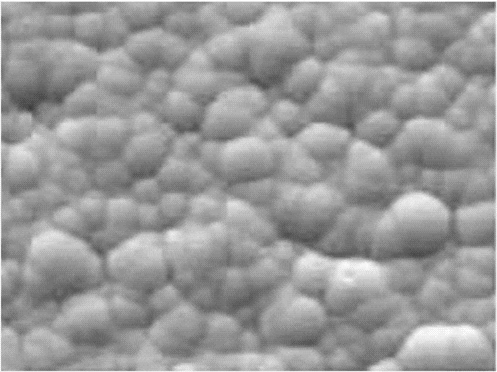
[0030] Such as figure 1 Shown is a schematic diagram of the nickel-immersion gold of the printed circuit board of the present invention. A kind of preparation method of the electroless nickel deposition of printed circuit board of the present invention comprises the following steps:
[0031] (1) The circuit board is pretreated; the pretreatment steps include grinding the board, sandblasting and baking the board. Grinding, roughening the surface of the copper plate, removing impurities and oxides on the copper surface, and increasing the bonding force of the plate surface; sandblasting, using the impact of high-speed sand flow to clean and roughen the surface of the plate, and performing two sandblasting treatments; The board is heated to eliminate the residual stress in the board. In the grinding plate, the grinding marks in the pretreatment step are 16mm.
[0032] (2) Upper board;
[0033] (3) Immerse the circuit board into the exchange tank, so that the board surface of ...
Embodiment 2
[0040] The difference between embodiment 2 and embodiment 1 is:
[0041] A kind of preparation method of the electroless nickel deposition of printed circuit board of the present invention comprises the following steps:
[0042] In step (1), in the grinding plate, the grinding marks in the pretreatment step are 14mm.
[0043] In step (3), the circuit board is immersed in the exchange tank to wet the surface of the circuit board; oil is removed to remove the oxide layer and oil stain on the surface of the circuit board; the dripping time of the exchange tank is 10 seconds.
[0044] In step (4), acid washing is used to clean the board surface of the circuit board with an acidic liquid; the acidic liquid is hydrochloric acid, the concentration range of the hydrochloric acid is 4%, and the temperature range is 43°C. The time for the activation treatment is 10 minutes.
[0045] In step (8), the thickness of the gold layer of the nickel-immersion gold is 0.05um.
Embodiment 3
[0047] The difference between embodiment 3 and embodiment 1 is:
[0048] In step (1), in the grinding plate, the grinding marks in the pretreatment step are 15mm.
[0049] In step (3), immerse the circuit board into the exchange tank to wet the surface of the circuit board; degrease, remove the oxide layer and oil stain on the circuit board surface; the dripping time of the exchange tank is ≤ 10 seconds.
[0050] In step (4), pickling is to use an acidic liquid to clean the surface of the circuit board; the acidic liquid is hydrochloric acid, the concentration range of the hydrochloric acid is 6%, and the temperature range is 40°C. The time of the activation treatment is 8 minutes.
[0051] In step (8), the thickness of the gold layer of the nickel-immersion gold is 0.12um.
PUM
 Abstract
Description
Claims
Application Information
 - R&D Engineer
- R&D Manager
- IP Professional
- Industry Leading Data Capabilities
- Powerful AI technology
- Patent DNA Extraction
Browse by: Latest US Patents, China's latest patents, Technical Efficacy Thesaurus, Application Domain, Technology Topic, Popular Technical Reports.
© 2024 PatSnap. All rights reserved.Legal|Privacy policy|Modern Slavery Act Transparency Statement|Sitemap|About US| Contact US: help@patsnap.com