Vertical double diffused field effect transistor and its manufacturing method

A field effect transistor, vertical double diffusion technology, applied in semiconductor/solid state device manufacturing, semiconductor devices, electrical components, etc., can solve problems affecting device performance, etc., to improve device performance, reduce on-resistance, and reduce resistance.

Inactive Publication Date: 2020-08-28
江苏清联光电技术研究院有限公司
View PDF4 Cites 0 Cited by
  • Summary
  • Abstract
  • Description
  • Claims
  • Application Information

AI Technical Summary

Problems solved by technology

However, N-type implantation is a full-chip implantation, and non-JFET regions will also be implanted, which will affect device performance.

Method used


Image

  • Vertical double diffused field effect transistor and its manufacturing method
  • Vertical double diffused field effect transistor and its manufacturing method
  • Vertical double diffused field effect transistor and its manufacturing method

Examples


Embodiment Construction

[0029] The following will clearly and completely describe the technical solutions in the embodiments of the present invention. Obviously, the described embodiments are only some of the embodiments of the present invention, rather than all the embodiments. Based on the embodiments of the present invention, all other embodiments obtained by persons of ordinary skill in the art without making creative efforts belong to the protection scope of the present invention.

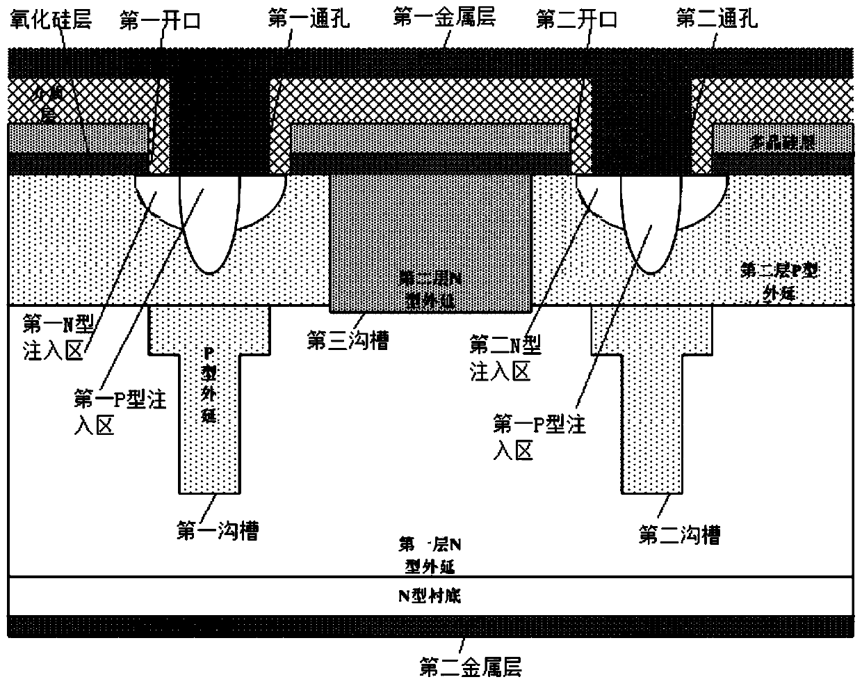
[0030] see figure 1 , figure 1 It is a schematic diagram of the cross-sectional structure of the vertical double-diffused field effect transistor provided by the present invention. The vertical double-diffused field effect transistor includes an N-type substrate, a first layer of N-type epitaxy formed on the N-type substrate, a first groove and a first layer of N-type epitaxial layer formed on the surface of the first layer of N-type epitaxial layer. Two trenches, the P-type epitaxy formed in the first trench and t...


PUM


Abstract

A vertical double diffusion field effect transistor comprises an N type substrate, first layers of N type extension, first grooves, second grooves, P type extension, second layers of P type extension,third grooves, second layers of P type extension, first N type injection areas, second N type injection areas, first P type injection areas, second P type injection areas, silicon oxide layers, polycrystalline silicon layers, medium layers, first through holes and second through holes, wherein the first grooves and the second grooves are formed in the surfaces of the first layers of N type extension, the P type extension is formed in the first grooves and the second grooves, the second layers of P type extension are formed on the first layers of N type extension and the P type extension, thethird grooves penetrate through the second layers of P type extension, the second layers of P type extension are located in the third grooves, the first N type injection areas and the second N type injection areas are located on the surfaces of the second layers of P type extension and correspond to the first grooves and the second grooves, the first P type injection areas and the second P type injection areas penetrate through the first N type injection areas and the second N type injection areas and extend to the second layers of P type extension, the silicon oxide layers and the polycrystalline silicon layers are formed sequentially, the medium layers are formed on the polycrystalline silicon layers, the first N type injection areas, the second N type injection areas and third injectionareas, the first through holes penetrate through the medium layers and correspond to the first N type injection areas and the first P type injection areas, and the second through holes penetrate through the medium layers and correspond to the second N type injection areas and the second P type injection areas.

Description

【Technical field】 [0001] The invention relates to the technical field of semiconductor chip fabrication, in particular to a vertical double diffused field effect transistor (VDMOS) and a fabrication method thereof. 【Background technique】 [0002] The drain and source poles of the vertical double diffused field effect transistor (VDMOS) are respectively on both sides of the device, so that the current flows vertically inside the device, increasing the current density, improving the rated current, and the on-resistance per unit area is also small, which is a A very versatile power device. The most important performance parameter of a vertical double diffused field effect transistor (VDMOS) is the operating loss, which can be divided into three parts: conduction loss, cut-off loss and switching loss. The conduction loss is determined by the conduction resistance, the cut-off loss is affected by the reverse leakage current, and the switching loss refers to the loss caused by th...

Claims


Application Information

Patent Timeline
Patent Type & Authority Patents(China)
IPC IPC(8): H01L29/78H01L21/336
CPCH01L29/66712H01L29/7802
Inventor 不公告发明人
Owner 江苏清联光电技术研究院有限公司
Why Eureka
Try Eureka