A kind of zn-sb-bi film material and preparation method thereof for multi-state phase change memory
A phase change memory, zn-sb-bi technology, applied in the field of phase change materials for information storage, can solve the problems of high energy, high power consumption, material stability and loss of phase change ability, etc., to reduce chemical bond energy, large crystal state Resistor, realize the effect of multi-bit multi-value storage
- Summary
- Abstract
- Description
- Claims
- Application Information
AI Technical Summary
Problems solved by technology
Method used
Image
Examples
Embodiment 1
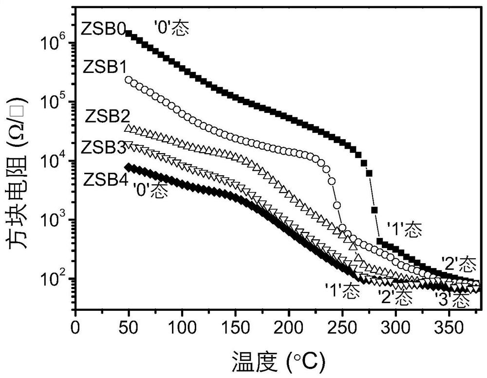
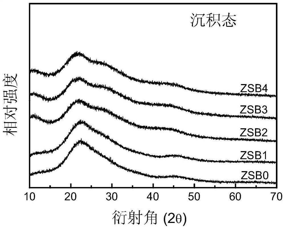
[0023] In the magnetron sputtering coating system, the quartz sheet or silicon oxide sheet is used as the substrate, the metal Bi single target is installed in the magnetron DC sputtering target, and the Zn 2 Sb 3 The alloy target is installed in the magnetron radio frequency sputtering target, and the sputtering chamber of the magnetron sputtering coating system is vacuumed until the vacuum degree of the chamber reaches 5.6×10 -4 Pa, and then pass high-purity argon gas with a volume flow rate of 50ml / min into the sputtering chamber until the air pressure in the sputtering chamber reaches the initiation pressure of 0.3 Pa required for sputtering, and then fix the Zn 2 Sb 3 The sputtering power of the target is 50 W, and the sputtering power of the metal Bi single target is adjusted to 0 W. The double target co-sputters the film at room temperature. After the sputtering thickness reaches 250 nm, the Zn-Sb phase change film in the deposited state is obtained. material whose ch...
Embodiment 2
[0026] The same as the first embodiment above, the difference is: during the sputtering process, the sputtering power of the metal Bi single target is controlled to 1 W, and the Zn 2 Sb 3 The sputtering power of the alloy target is 50 W, and the double-target co-sputtering coating is carried out at room temperature. After the sputtering thickness is 250 nm, the as-deposited Zn-Sb-Bi phase-change thin film material is obtained, and its chemical structure is (Zn 2 Sb3 ) 96.8 Bi 3.2 .
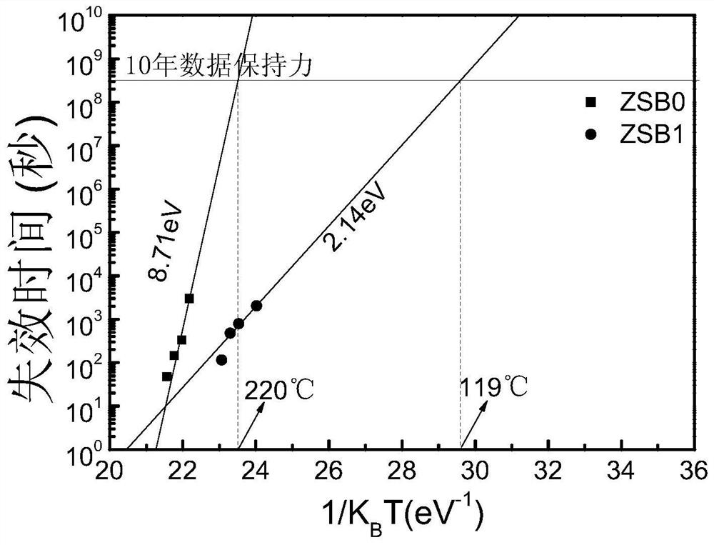
[0027] The prepared thin film material is carried out in-situ resistance and XRD test, find out that the performance index of the thin film prepared in this embodiment is as follows: crystallization temperature T c It is 229 ℃, the phase transition temperature is 320 ℃, the crystallization activation energy is 2.14 eV, the ten-year data retention temperature is 119 ℃, and it has 3 kinds of resistance states.
Embodiment 3
[0029] Same as the first embodiment above, the difference is: during the sputtering process, the sputtering power of the metal Bi single target is controlled to 2 W, and the Zn 2 Sb 3 The sputtering power of the alloy target is 50 W, and the double-target co-sputtering coating is carried out at room temperature. After the sputtering thickness is 250 nm, the deposited Zn-Sb-Bi thin film material is obtained, and its chemical structure is (Zn 2 Sb 3 ) 94.6 Bi 5.4 .
[0030] The prepared thin film material is carried out in-situ resistance and XRD test, find out that the performance index of the thin film prepared in this embodiment is as follows: crystallization temperature T c It is 163 ℃ and has 4 kinds of resistance states.
PUM
| Property | Measurement | Unit |
|---|---|---|
| melting point | aaaaa | aaaaa |
| crystallization temperature | aaaaa | aaaaa |
| phase transition temperature | aaaaa | aaaaa |
Abstract
Description
Claims
Application Information
 - R&D
- Intellectual Property
- Life Sciences
- Materials
- Tech Scout
- Unparalleled Data Quality
- Higher Quality Content
- 60% Fewer Hallucinations
Browse by: Latest US Patents, China's latest patents, Technical Efficacy Thesaurus, Application Domain, Technology Topic, Popular Technical Reports.
© 2025 PatSnap. All rights reserved.Legal|Privacy policy|Modern Slavery Act Transparency Statement|Sitemap|About US| Contact US: help@patsnap.com


