Manufacturing method of metal lines distributed on different orientation surfaces of insulator
A technology of metal circuit and manufacturing method, which is applied in the direction of printed circuit manufacturing, removal of conductive materials by chemical/electrolytic methods, printed circuit, etc., to achieve the effect of small change in surface roughness of the bracket, low surface roughness, and high connection reliability
- Summary
- Abstract
- Description
- Claims
- Application Information
AI Technical Summary
Problems solved by technology
Method used
Image

Examples
Embodiment 1
[0062] On the basis of the above non-limiting embodiments, this embodiment provides a method for manufacturing a metal circuit on a small insulator, and the specific manufacturing method is as follows:
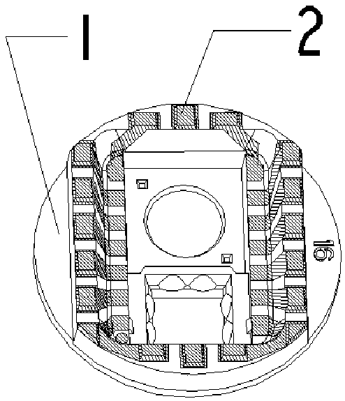
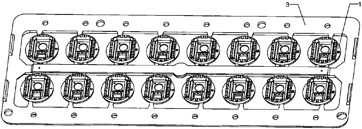
[0063] A1. making the insulator support 1 of the metal circuit;
[0064] A2. Copper is sputtered on the surface of the insulator support 1 and the frame 3 as a bottom metal;
[0065] A3. Electroplate copper on the underlying metal, thicken until the thickness of the copper plating is equal to or slightly greater than the line requirements;
[0066] A4. Electroplate a tin-lead alloy on the surface of the copper plating layer as a resist layer for subsequent chemical etching of copper;
[0067] A5. Use a laser to ablate the tin-lead alloy along the outer contour of each metal line until the copper coating under the tin-lead alloy coating is exposed. The ablation depth is greater than the tin-lead alloy layer but less than the copper coating. The width of the ablation groove is ...
Embodiment 2
[0076] On the basis of the above-mentioned non-limiting embodiments, this embodiment further provides a method for manufacturing metal lines distributed on the surface of the insulator in different orientations, the method specifically includes:
[0077] B1. Carrier insulator support for making metal lines;
[0078] B2. Sputter copper plating on the surface of the insulator bracket and frame as the underlying metal;
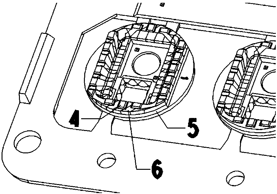
[0079] B3. ablate the underlying metal along the outer contour of the metal circuit 13.1 and the electroplating lead 13.2 with a laser, and divide the underlying metal on the insulator support into a circuit area 13 and a non-circuit area 14 that include the metal circuit and its electroplating lead and are electrically insulated from each other, Such as Figure 9 shown;
[0080] B4. electroplating copper and tin-lead on the line area 13, the thickness of the copper coating needs to reach the required thickness of the line, and the metal on the insulator suppor...
PUM
 Abstract
Description
Claims
Application Information
 - Generate Ideas
- Intellectual Property
- Life Sciences
- Materials
- Tech Scout
- Unparalleled Data Quality
- Higher Quality Content
- 60% Fewer Hallucinations
Browse by: Latest US Patents, China's latest patents, Technical Efficacy Thesaurus, Application Domain, Technology Topic, Popular Technical Reports.
© 2025 PatSnap. All rights reserved.Legal|Privacy policy|Modern Slavery Act Transparency Statement|Sitemap|About US| Contact US: help@patsnap.com