Black phosphorus based p-n photodetector
A photoelectric detector, black phosphorus technology, applied in the direction of circuits, electrical components, semiconductor devices, etc., can solve the problem that the cut-off wavelength cannot be extended
- Summary
- Abstract
- Description
- Claims
- Application Information
AI Technical Summary
Problems solved by technology
Method used
Image
Examples
Embodiment
[0020] Embodiment: Fabrication and analysis of photodetectors based on black phosphorus (BP).
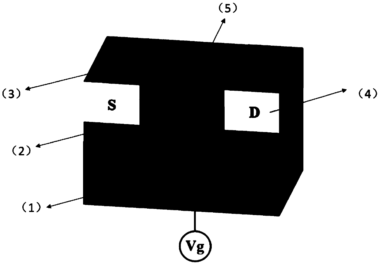
[0021] refer to figure 1 , the implementation steps of this example are as follows:
[0022] Step 1: Doping the substrate to make a buried layer.
[0023] Firstly, the substrate is doped by ion implantation process. The temperature of the silicon substrate 1 is controlled at room temperature to avoid thermal defects caused by high-temperature diffusion, and boron doping is performed to obtain a P-type silicon substrate 1 . Then use the thermal oxidation process, the method of combining dry and wet oxygen, and grow SiO at a temperature of 900 degrees. 2 The thickness of the oxide mask layer 2 is controlled at 50nm.
[0024] Step 2: Depositing Black Phosphorus
[0025] A layer of black phosphorus was deposited on the oxide mask layer by magnetron sputtering in physical vapor deposition, with a gas pressure of 2 millitorr and a deposition temperature of 110 degrees for 80 minutes....
PUM
 Abstract
Description
Claims
Application Information
 - R&D
- Intellectual Property
- Life Sciences
- Materials
- Tech Scout
- Unparalleled Data Quality
- Higher Quality Content
- 60% Fewer Hallucinations
Browse by: Latest US Patents, China's latest patents, Technical Efficacy Thesaurus, Application Domain, Technology Topic, Popular Technical Reports.
© 2025 PatSnap. All rights reserved.Legal|Privacy policy|Modern Slavery Act Transparency Statement|Sitemap|About US| Contact US: help@patsnap.com


