
IGBT chip manufacturing method and IGBT chip

A manufacturing method and chip technology, which is applied in semiconductor/solid-state device manufacturing, electrical components, circuits, etc., can solve problems such as prone to dynamic latch-up, and achieve the effect of improving anti-latch-up ability and improving anti-latch-up ability

Active Publication Date: 2018-01-12
GLOBAL ENERGY INTERCONNECTION RES INST CO LTD
View PDF3 Cites 0 Cited by
  • Summary
  • Abstract
  • Description
  • Claims
  • Application Information

AI Technical Summary

Problems solved by technology

[0004] In view of this, an embodiment of the present invention provides a method for manufacturing an IGBT chip and an IGBT chip to solve the problem in the prior art that the IGBT chip is prone to dynamic latch-up during the over-current shutdown process

Method used


Image

  • IGBT chip manufacturing method and IGBT chip
  • IGBT chip manufacturing method and IGBT chip
  • IGBT chip manufacturing method and IGBT chip

Examples


Embodiment Construction

[0033] In order to make the purpose, technical solutions and advantages of the embodiments of the present invention clearer, the technical solutions in the embodiments of the present invention will be clearly and completely described below in conjunction with the drawings in the embodiments of the present invention. Obviously, the described embodiments It is a part of embodiments of the present invention, but not all embodiments. Based on the embodiments of the present invention, all other embodiments obtained by those skilled in the art without creative efforts fall within the protection scope of the present invention.

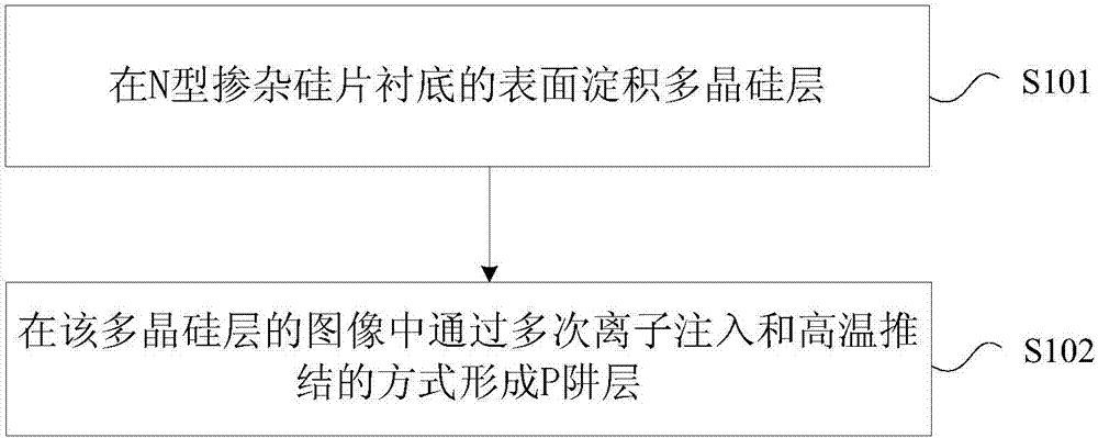
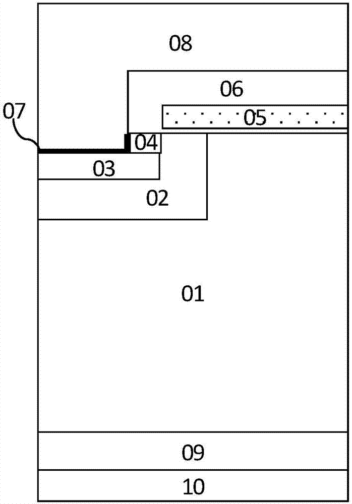
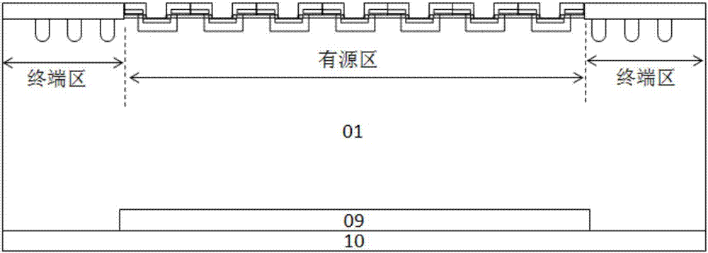
[0034] In this embodiment, a method for manufacturing an insulated gate bipolar transistor IGBT chip is provided, figure 1 is a flow chart of the method for manufacturing an IGBT chip according to an embodiment of the present invention, such as figure 1 As shown, the process includes the following steps:

[0035] Step S101, depositing a polysilicon layer on...


PUM


Abstract

The invention provides an IGBT chip manufacturing method and an IGBT chip. The IGBT chip manufacturing method includes depositing a polysilicon layer on the surface of an N-type doped silicon wafer substrate; and forming a P-well layer in the pattern of the polysilicon layer by means of multitime ion implantation and high temperature pushing. The P-well layer is formed by means of multitime ion implantation and high temperature pushing, in this way, the P well under the N area has higher concentration, and the improvement of the latching capability is facilitated, so that the problem that theIGBT chip in the prior art is easy to occur dynamic latching in the overcurrent turn-off process, the anti-latching capability of the IGBT in the overcurrent turn-off process is improved, and meanwhile, the back side adopts the local doping or oxide isolation manner, the current concentration of the active region edge is reduced, and the overcurrent turn-off capability of the IGBT is improved.

Description

technical field [0001] The invention relates to the technical field of power semiconductor devices, in particular to an IGBT chip manufacturing method and the IGBT chip. Background technique [0002] Due to the advantages of low switching loss, simple gate control, and excellent switch controllability, the insulated gate bipolar transistor (Insulated Gate Bipolar Transistor, referred to as IGBT) is widely used in industrial frequency conversion, high-power locomotive traction, and power grids. Since its invention in the 1980s, the vertical structure of IGBT has undergone development from punch-through type, non-punch-through type to soft punch-through type, and the power density that can be handled by a chip per unit area is increasing. Especially for IGBT chips using transparent collector technology, since there is no need to use carrier lifetime control technology, the on-state voltage drop has a positive temperature coefficient, which is easy to realize the parallel use o...

Claims


Application Information

Patent Timeline
Patent Type & Authority Applications(China)
IPC IPC(8): H01L21/331H01L29/06H01L29/739
Inventor 王耀华温家良金锐赵哿刘江高明超崔磊李立朱涛
Owner GLOBAL ENERGY INTERCONNECTION RES INST CO LTD
Learn More