
Anti-latch insulated gate bipolar transistor device

A bipolar transistor, insulated gate technology, applied in semiconductor devices, electrical components, circuits, etc., can solve problems such as limitations, increased manufacturing costs, process control, and implementation complexity and difficulty, to suppress forward bias and improve robustness. performance, improving the effect of latch-up resistance

Active Publication Date: 2020-06-02
INST OF MICROELECTRONICS CHINESE ACAD OF SCI
View PDF4 Cites 0 Cited by
  • Summary
  • Abstract
  • Description
  • Claims
  • Application Information

AI Technical Summary

Problems solved by technology

Although this method can improve the IGBT latch-up characteristics to a certain extent, in terms of technology, it is necessary to accurately realize the lateral diffusion of P+ to the bottom of the N+ emitter without affecting the junction depth and doping concentration of the N+ emitter; The doping concentration and morphology of the P-base region at the surface channel of the IGBT will not affect the threshold characteristics of the IGBT device, which has certain complexity and difficulty in process control and implementation, and will also increase the manufacturing cost
At the same time, with the continuous improvement of IGBT performance, the chip is getting thinner and the current density is getting higher and higher, and the requirements for the device's ability to resist latch-up current are getting higher and higher. However, the above-mentioned traditional methods have been limited in improving the device's latch-up current density.

Method used


Image

  • Anti-latch insulated gate bipolar transistor device
  • Anti-latch insulated gate bipolar transistor device
  • Anti-latch insulated gate bipolar transistor device

Examples


Embodiment Construction

[0044] In order to make the object, technical solution and advantages of the present invention clearer, the present invention will be further described in detail below in conjunction with specific embodiments and with reference to the accompanying drawings.

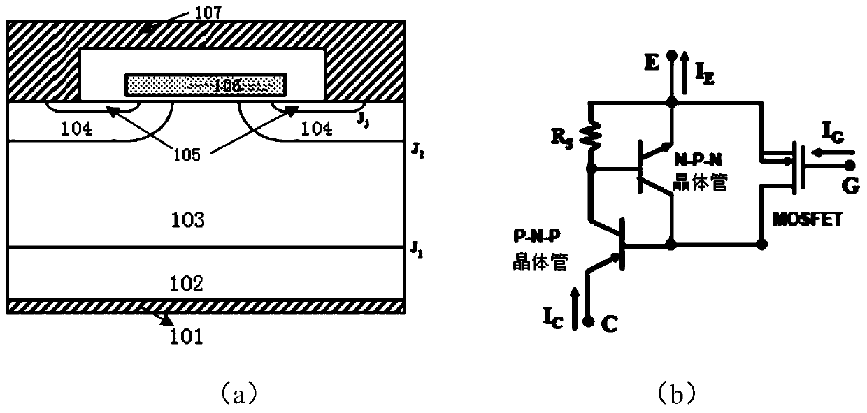
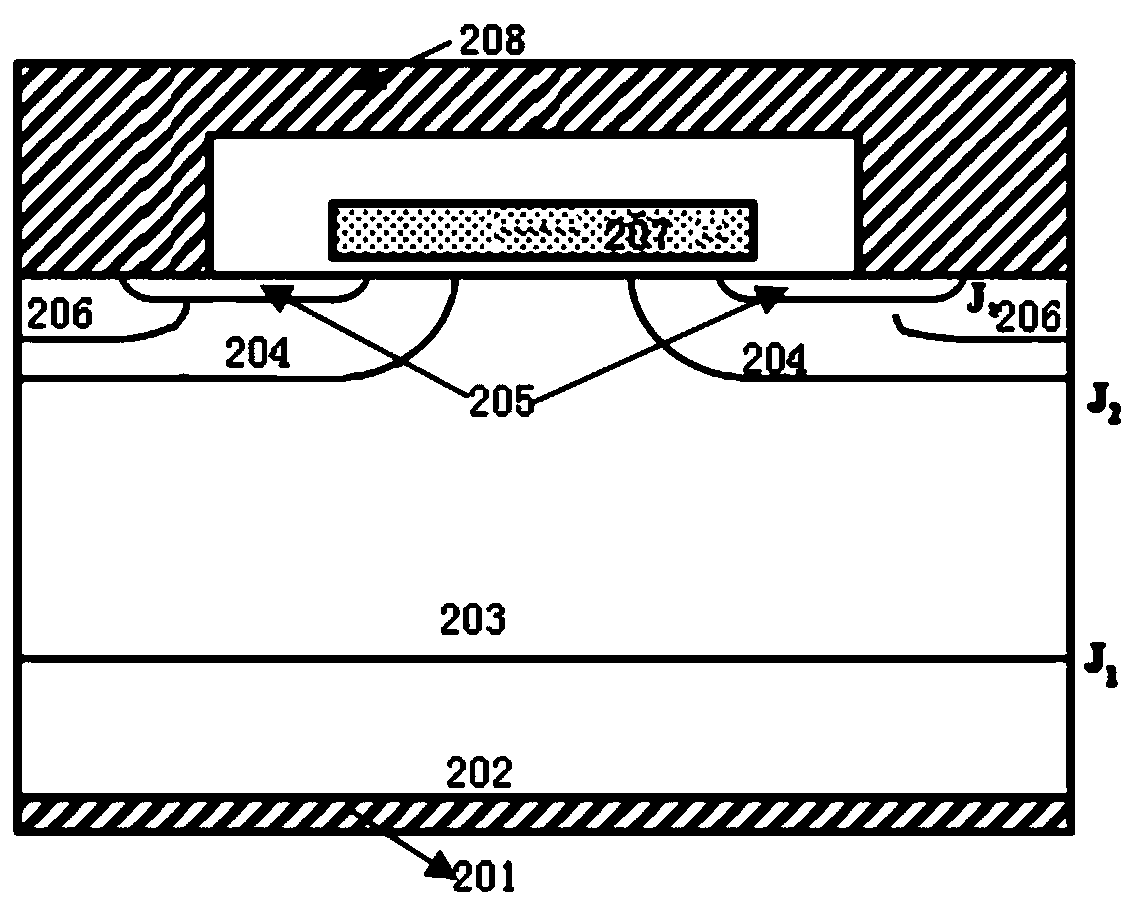
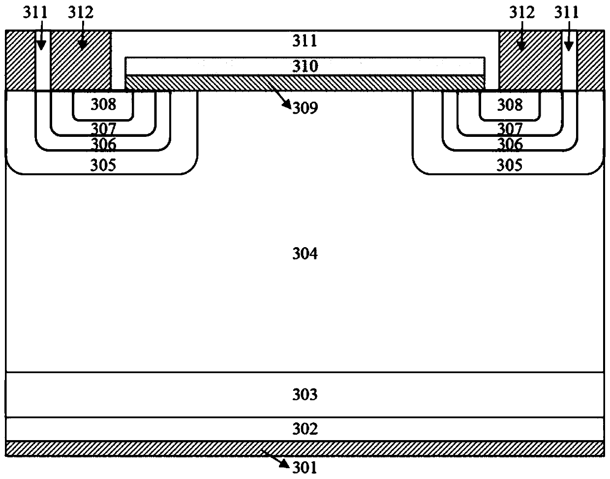
[0045] The invention discloses an anti-latch insulated gate bipolar transistor device. The anti-latch-up insulated gate bipolar transistor device includes: a P-type heavily doped collector region; an N-type field stop layer; an N-type lightly doped drift layer; a P-type Base region located in the drift layer; The annular N-type doped buried layer in the base region; the N+ emitter region; the emitter metal; the gate dielectric layer; the gate on the gate dielectric layer; the interlayer dielectric. Among them, the annular N-type doped buried layer surrounds the N+ emitter region in the p-base region, one end is connected to the channel, and the other end is connected to the interlayer medium on the surface, physically div...


PUM


Abstract

The invention discloses an insulated gate bipolar transistor which comprises a grid, a collector, two emitters and an annular N-type doped buried layer, the two emitters are located on corresponding N+ emitter regions and part of p-type base regions respectively, the p-type base regions are located in an N-type lightly doped drift layer, and the two N + emitter regions are located in the p-type base regions; and the annular N-type doped buried layer surrounds the N + emitter regions in the p-type base region, one end of the annular N-type doped buried layer is connected with a channel, the other end of the annular N-type doped buried layer is connected with an interlayer dielectric on the surface, and the annular N-type doped buried layer physically divides the p-type base region into a p-type base region 1 and a p-type base region 2. According to the invention, hole current can be effectively prevented from flowing through an area below the N + emitter but electrons moving along thechannel are not influenced, so that electron current and hole current are separated, current flowing under the N + emitter is greatly reduced, positive bias of the p-base region / N + emitter junction is inhibited, latch-up resistance of the device is remarkably improved, and firmness of the device is improved.

Description

technical field [0001] The invention relates to the technical field of semiconductor devices, in particular to an anti-latch insulated gate bipolar transistor device. Background technique [0002] Insulated Gate Bipolar Transistor IGBT (INsulated Gate Bipolar TraNsistor) is a new type of high-power device. It combines the characteristics of MOSFET gate voltage control and the low on-resistance of bipolar transistors, and improves the interaction between the withstand voltage and on-resistance of the device. In the case of pinning, it has the advantages of high voltage, high current, high power integration density, large input impedance, small on-resistance, and low switching loss. It has gained wide application space in many fields such as frequency conversion home appliances, industrial control, electric and hybrid vehicles, new energy, and smart grid. [0003] In practical applications, many requirements are put forward for IGBT. In addition to high performance such as lo...

Claims


Application Information

Patent Timeline
Patent Type & Authority Applications(China)
IPC IPC(8): H01L29/739H01L29/06H01L29/10
CPCH01L29/7395H01L29/0684H01L29/1004
Inventor 田晓丽冯旺杨雨陆江白云刘新宇
Owner INST OF MICROELECTRONICS CHINESE ACAD OF SCI
Learn More