A fully self-aligned insulated gate bipolar transistor device and its manufacturing method
A bipolar transistor, self-aligned technology, applied in semiconductor/solid-state device manufacturing, electrical components, circuits, etc., can solve problems such as unreasonable device structure, hidden dangers of devices, affecting device operating parameters and reliability, etc., and achieve process steps Reduced, increased steps, effects of latch-up improvement
- Summary
- Abstract
- Description
- Claims
- Application Information
AI Technical Summary
Problems solved by technology
Method used
Image

Examples
Embodiment 1
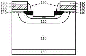
[0069] like figure 1 As shown, it is a fully self-aligned insulated gate bipolar transistor device, including a first conductivity type substrate 110, a second conductivity type base region 120 is disposed in the first main surface of the first conductivity type substrate 110, A second conductivity type deep diffusion region 130 is provided in the second conductivity type base region 120, and the second conductivity type deep diffusion region 130 is in a “concave” shape. region 140, the emitter region 140 of the first conductivity type is respectively arranged on the two convex parts of the "concave" type of the deep diffusion region 130 of the second conductivity type, and a grid is arranged on the first main surface of each emitter region 140 of the first conductivity type Pole insulating layer 160, a polysilicon gate layer 170 is provided on the gate insulating layer 160, a second insulating layer 180 is provided on the polysilicon gate layer 170, insulating sidewalls 190 ...
Embodiment 2
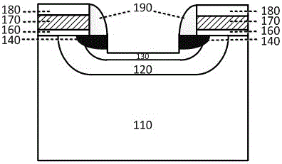
[0099] like figure 1 As shown, it is a fully self-aligned insulated gate bipolar transistor device, including a first conductivity type substrate 110, and a second conductivity type base region 120 is arranged in the first main surface of the first conductivity type substrate 110, The second conductivity type base region 120 is provided with a second conductivity type deep diffusion region 130, the second conductivity type deep diffusion region 130 is in a "concave" shape, and the second conductivity type base region 120 is provided with a first conductivity type emitter Region 140, the first conductivity type emitter region 140 is respectively disposed on the two convex portions of the "concave" type of the second conductivity type deep diffusion region 130, and a gate is provided on the first main surface of each first conductivity type emitter region 140 The polar insulating layer 160, the gate insulating layer 160 is provided with a polysilicon gate layer 170, the polysil...
Embodiment 3
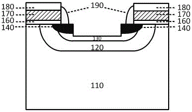
[0101] like figure 1 As shown, it is a fully self-aligned insulated gate bipolar transistor device, including a first conductivity type substrate 110, and a second conductivity type base region 120 is arranged in the first main surface of the first conductivity type substrate 110, The second conductivity type base region 120 is provided with a second conductivity type deep diffusion region 130, the second conductivity type deep diffusion region 130 is in a "concave" shape, and the second conductivity type base region 120 is provided with a first conductivity type emitter Region 140, the first conductivity type emitter region 140 is respectively disposed on the two convex portions of the "concave" type of the second conductivity type deep diffusion region 130, and a gate is provided on the first main surface of each first conductivity type emitter region 140 The polar insulating layer 160, the gate insulating layer 160 is provided with a polysilicon gate layer 170, the polysil...
PUM
 Abstract
Description
Claims
Application Information
 - Generate Ideas
- Intellectual Property
- Life Sciences
- Materials
- Tech Scout
- Unparalleled Data Quality
- Higher Quality Content
- 60% Fewer Hallucinations
Browse by: Latest US Patents, China's latest patents, Technical Efficacy Thesaurus, Application Domain, Technology Topic, Popular Technical Reports.
© 2025 PatSnap. All rights reserved.Legal|Privacy policy|Modern Slavery Act Transparency Statement|Sitemap|About US| Contact US: help@patsnap.com